This engineering case study reviews a complex 24-layer, 3.0mm thick FR-4 TG170 board intended for high-reliability applications. With 0.5oz/1oz copper, ENIG finish, impedance control, and multiple press-fit holes plus backdrilled vias in BGA areas, the design pushed several manufacturing limits during our CAM review.
Heavy boards with deep backdrills, tight press-fit tolerances, and conflicting via plugging requirements frequently trigger extensive engineering questions (EQs). Our CAM team identified over 20 issues ranging from drill compensation to copper balance and process compatibility. Early clarification prevented potential scrap, yield loss, and reliability failures.
3mm 24-Layer FR4 PCB Order Specifications and Key Features
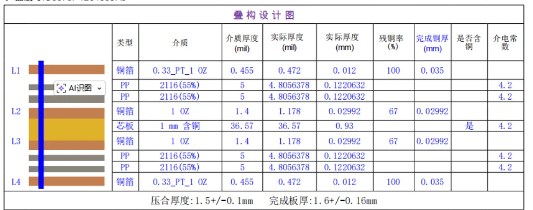
This was a 24-layer rigid PCB (FR4-20260309-026) fabricated on FR-4 TG170 material with a finished board thickness of 3.0mm. Outer layers used 1oz copper, inner layers 0.5oz. The single board size measured 279.7 × 215.57mm, delivered as individual pieces (no panelization beyond 1×1). Surface finish was ENIG, with full red solder mask on both sides and white silkscreen. Minimum hole size was specified at 0.4mm, with 100% flying probe testing required.
Key challenges included multiple press-fit connector holes with strict finished diameter, copper thickness, nickel thickness, and gold thickness requirements, extensive backdrilling (including maximum stub length of 4mil), resin-plugged vias (especially in BGA regions), and impedance-controlled stackup. Total copper weight and aspect ratio on a 3.0mm board made drillability, plating uniformity, and warpage control particularly demanding.
Critical PCB CAM Issues Found in 24-Layer Thick Board Review
1. Press-Fit Holes: Drill Size, Finished Diameter & Plating Control Challenges
The customer provided detailed requirements for four different press-fit hole types, including finished hole diameters, hole copper thickness (25μm minimum), nickel thickness, and gold thickness. Our engineer noticed that the requested drill sizes, after metric conversion, did not align consistently with our standard compensation rules for the different hole categories.
We also observed that the design specified backdrilling on some press-fit locations with a maximum 4mil stub. Our CAM team flagged this immediately: ''We noticed the backdrill stub requirement of 4mil was extremely aggressive for a 3.0mm board. Controlling residual stub length to such tight tolerance while maintaining plating integrity is very difficult and risks via cracking or inconsistent impedance."
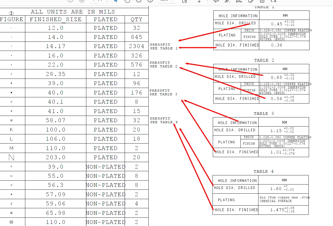
Figure 1 Customer's requirements for press-fit holes
If ignored, backdrill depth variation could easily exceed the 4mil limit, leading to excessive stub length, signal reflections, and potential signal integrity failure in high-speed applications. Conversely, over-drilling risks breaking through the opposite side or causing copper peeling at the knee of the via.
2. Backdrill Depth Control and Residual Stub Length on 3mm Multilayer PCB
Multiple backdrilled vias were specified with maximum depth limits. Our standard backdrill tool sizes did not match some of the requested hole diameters, and the tight depth tolerance posed significant process risk on a thick multilayer board.
Our engineer confirmed: ''After reviewing the stackup and drill files, we found the backdrill hole sizes fell outside our preferred tooling library. We recommended confirming acceptable finished diameters and whether residual copper thickness (backdrill clearance to opposite pad) had specific requirements." Ignoring this could result in drill breakout, incomplete copper removal, or damage to adjacent layers, causing open circuits or delamination during assembly.
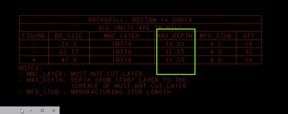
Figure 2 Strict requirements for back drill
3. Via Resin Plugging Conflicts with Solder Mask Windows in BGA Areas
The order required resin plugging and planarization for vias, yet the solder mask design included small openings (windows) on the bottom side for some vias. Additionally, many backdrilled vias were located in BGA regions.
We pointed out: ''Our engineer identified that vias with bottom-side solder mask windows cannot be reliably resin-plugged because ink will flow into the holes during mask application, causing blockages. For BGA-area backdrilled vias, we must follow resin plug process per Gerber but ensure compatibility with the customer's plugging intent."
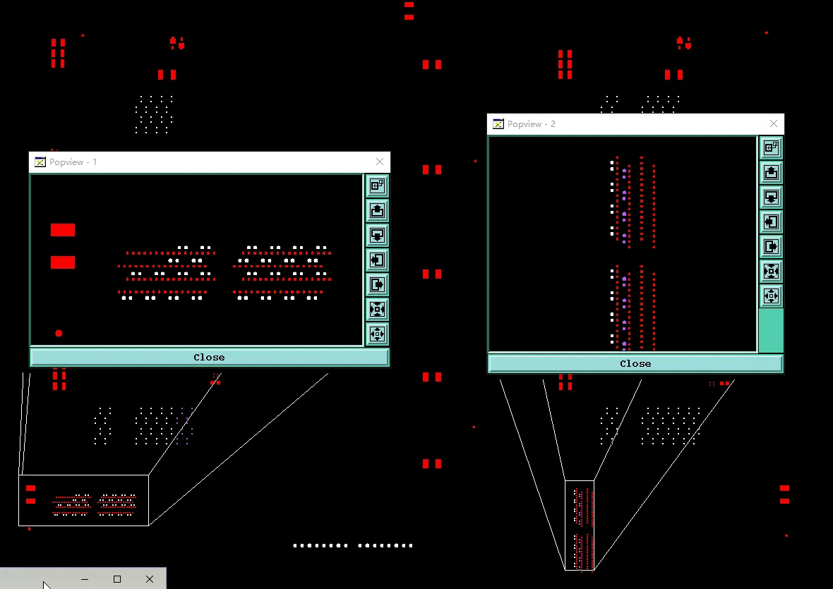
Figure 3 backdrilled vias were located in BGA regions
If unresolved, this mismatch would lead to either plugged vias with mask ink intrusion (poor planarity and solderability) or unplugged vias causing solder wicking, shorts during BGA assembly, or reliability failures under thermal cycling.
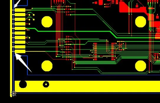
4. Copper Balance, Warpage Risk & Solder Mask Opening Design on Thick Boards
Top and bottom layer copper densities differed significantly. Combined with the 3.0mm thickness and TG170 material, this created high warpage risk. Additionally, solder mask opening lines were designed at 20mil width, far exceeding our standard 6mil, and some openings were not aligned with the board outline.
Our CAM engineer noted: ''We noticed the TL/BL copper imbalance was substantial. Without adjustment, the finished board would likely exhibit excessive bow and twist, failing IPC-6012 Class 2 flatness requirements. We suggested adding balanced copper on the BL side connected to GND where possible."
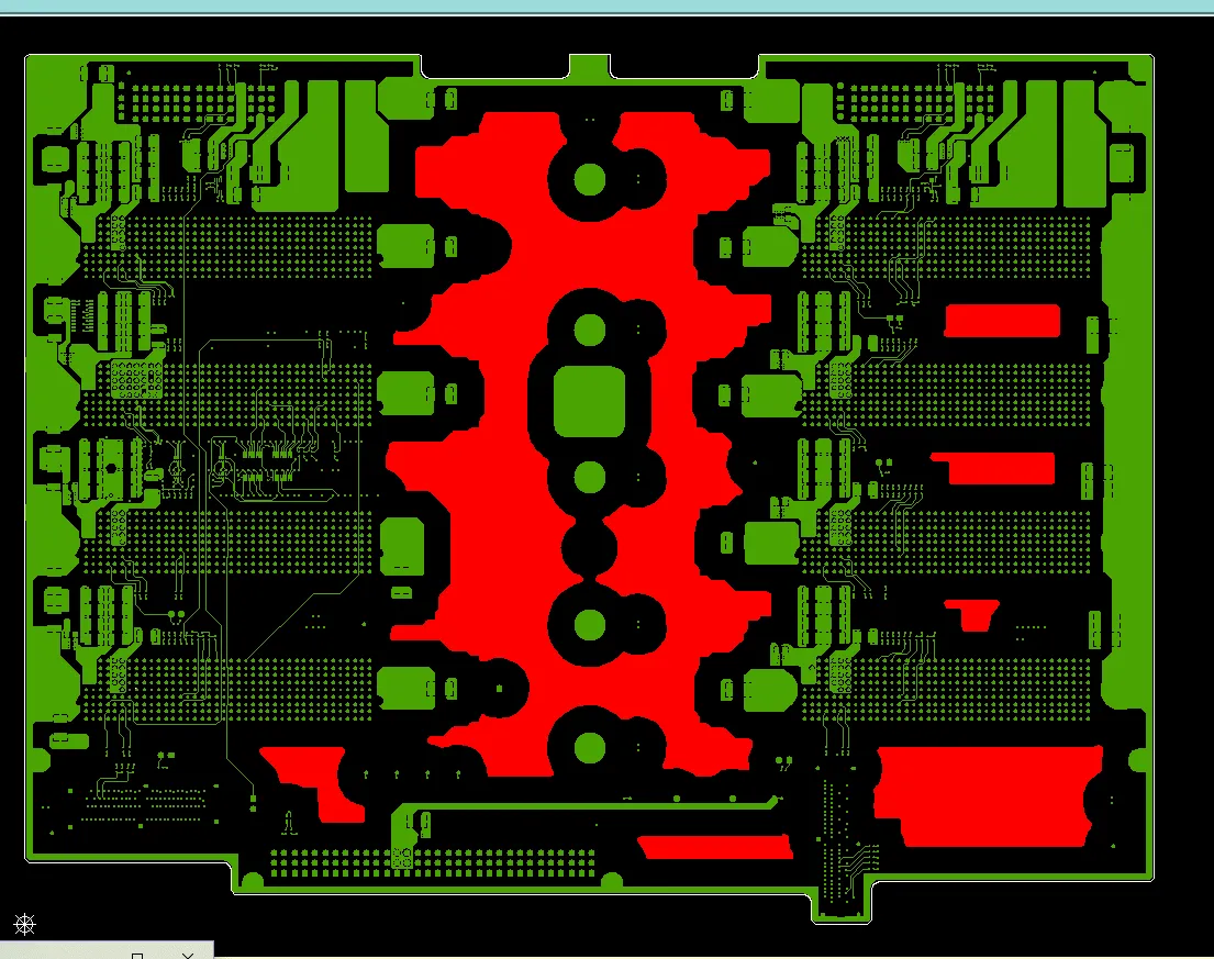
Figure 4 copper balance, board warpage risk
The wide solder mask openings risked exposing a ring of substrate at the board edge after routing. If produced as-is, this would cause cosmetic defects, potential edge shorting after depanelization (even though single piece), and reduced edge insulation reliability.
5. Additional CAM Concerns: Silkscreen, Tolerances & Process Compatibility
Several silkscreen elements connected to pads or frames risked blurring or incomplete legend after printing. Board thickness tolerance was specified very tightly, difficult to hold consistently on a 24-layer build. Press-fit hole tolerances conflicted across EQ replies. No process edge was specified, yet batch/SN marking was requested on process edge. Minimum hole size in fabrication notes did not match actual drill files.
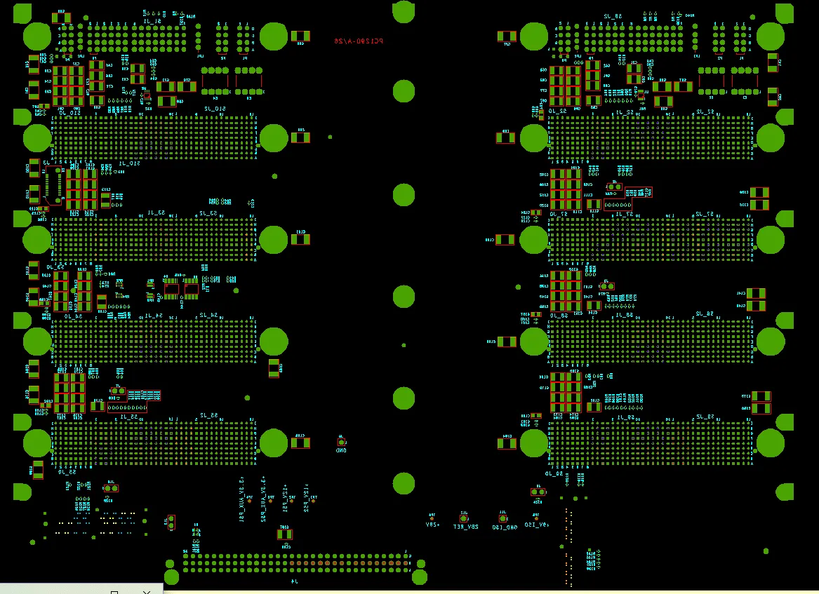
Figure 5 Non-compliant silkscreen design
We also confirmed material and solder mask color had no UL certification available for the chosen combination.
Major DFM Risks for Backdrilling and Press-Fit in 24-Layer 3mm FR4 PCBs
This case highlights several recurring DFM pitfalls in high-layer-count thick boards:
- Press-fit holes require clear distinction between drill size and finished hole diameter. Unclear compensation leads to out-of-tolerance holes and assembly failures.
- Backdrill stub length under 5mil on thick boards is extremely challenging and often requires design compromise to avoid via reliability issues.
- Via plugging specifications must be consistent with solder mask design. Conflicting requirements cause ink intrusion or insufficient filling.
- Copper balance is critical on multilayer boards >2.5mm thick. Large density differences almost guarantee warpage, leading to assembly problems and scrap.
- Solder mask opening design near board edges must consider routing clearance to prevent base material exposure.
Ignoring these would have resulted in high scrap rate, multiple production delays, and potential field failures from poor signal integrity or mechanical stress.
| Issue | Primary Risk | Resolution Applied |
|---|---|---|
| Press-Fit Hole Tolerances | Inconsistent drill vs finished diameter after compensation | Adjusted compensation per factory standards with customer approval |
| Backdrill Stub Length | 4mil tolerance difficult on 3mm board | Relaxed to achievable value while maintaining signal integrity |
| Via Plugging & Solder Mask | Ink intrusion from windows on plugged vias | Standardized resin plug where compatible, documented BGA process |
| Copper Imbalance | Warpage exceeding IPC limits | Added balanced GND copper on bottom layer |
Table 1: Key Manufacturing Risks and Resolutions in 24-Layer 3mm FR4 PCB
Reviewing these elements during CAM helps align design with production realities for high-reliability boards.
Collaborative Resolution of Press-Fit, Backdrill & Copper Balance EQs
Our team worked closely with the customer through multiple rounds of clarification. We adjusted drill compensation for press-fit holes based on our proven manufacturing capability, relaxed backdrill stub to a mutually acceptable value, and standardized via plugging process to resin plug where solder mask allowed, with clear documentation for BGA areas.
Copper balancing was implemented on the bottom layer with customer-approved GND connections. Solder mask openings were optimized to 6-8mil with proper alignment. Board thickness tolerance was adjusted to a realistic range per IPC-6012. Silkscreen was reviewed and optimized to prevent bridging. All markings were placed on the board proper since no process edge was used.
''After final file confirmation and stackup review, our CAM engineer approved the production data with all modifications documented," the team recorded.
Production Outcome After Iterative EQ Clarifications
All engineering questions were resolved through iterative clarification and data optimization. The production files were released with adjusted parameters that balanced customer requirements against manufacturing capability. The order proceeded to fabrication with significantly reduced risk of defects.
DFM Best Practices for High-Layer Thick FR4 PCBs with Backdrills
- Clearly specify whether hole sizes in drawings are drill or finished diameters, especially for press-fit connectors.
- Provide realistic backdrill stub requirements (typically ≥5-6mil for thick boards) and confirm tooling compatibility early.
- Ensure via plugging requirements match solder mask design — avoid windows on plugged vias.
- Maintain reasonable copper density balance between layers on thick multilayer boards.
- Use standard solder mask opening widths (6-8mil) and align them properly with board outline.
- Coordinate legend placement away from pads and frames to prevent printing defects.
- Include complete stackup and impedance information with clear reference layers.
- Verify material and color combinations against UL certification needs before finalizing design.
FAQ
Q1: Why is controlling backdrill stub to 4mil very difficult on a 3.0mm 24-layer board?
A1: Depth control tolerance accumulates from material variation, drill wear, and machine repeatability. On thick boards, even small variations can exceed 4mil, risking either excessive stubs (signal issues) or over-drilling (reliability failure).
Q2: Can vias with solder mask windows on one side be resin plugged?
A2: Generally no. The window allows mask ink to enter the hole during application, defeating the purpose of plugging and causing planarity or contamination issues.
Q3: Why must copper balance be addressed on thick multilayer PCBs?
A3: Uneven copper distribution causes differential shrinkage during lamination and cooling, resulting in warpage that exceeds IPC specifications and complicates SMT assembly.
Q4: What happens if press-fit hole tolerances are not clearly defined?
A4: Finished holes may fall outside the connector manufacturer’s acceptance range, leading to poor press-fit retention, damaged connectors, or open circuits after assembly.
Q5: Why do factories prefer standard solder mask opening widths near board edges?
A5: Wide openings (e.g. 20mil) combined with routing tolerance often expose base material, creating cosmetic defects and potential electrical weakness at the edge.
Q6: Is it necessary to connect added balancing copper to GND?
A6: Yes, floating copper islands can cause etching issues, plating anomalies, or signal interference. Connecting to GND ensures electrical integrity and manufacturing stability.