In high-frequency PCB production, even seemingly straightforward orders can hide significant manufacturability risks. This case involves a 4-layer hybrid Rogers design (RO4003C + RO4350B) ordered for RF application, with blind vias, V-CUT panelization, and specific no-solder-mask requirements. During our CAM engineering review, multiple conflicts between design intent and production capability surfaced, requiring detailed clarification with the customer.
As a senior CAM engineer with over 15 years in RF PCB fabrication, I always emphasize that early engineering questions (EQs) prevent scrap, delays, and performance issues. In this project, we addressed stackup asymmetry, blind via spacing violations, solder mask conflicts, V-CUT copper clearance, and several other critical details. Ignoring these would have led to warpage, breakout, exposed copper, or short circuits.
Order Overview
This was a 4-layer high-frequency PCB (#ROG-20251219-001), panelized 2x2, with final board size approximately 53 × 81 mm. The customer specified Rogers RO4350B material, TG >280°C, 1.5 mm finished thickness, and ENIG surface finish. Copper weights were 0.5 oz outer / 1 oz inner, with minimum hole size 0.4 mm and trace/space at 4 mil. The order included 40 pieces (10 sets), 100% electrical testing, resin plugging for small vias and blind vias, and V-CUT depanelization.
Notably, the stackup involved a hybrid construction: layers 1-2 using RO4003C (0.203 mm core) and layers 3-4 using RO4350B (0.76 mm), with specific Shengyi PP. The design included 1-2 blind vias (0.25 mm), no gold fingers despite a noted bevel requirement, and explicit instructions for no solder mask with characters printed directly on the gold surface. Delivery was requested within 12 days.
Such hybrid RF boards are common in high-performance applications but demand precise DFM validation due to differing material properties and processing sensitivities.
Main Engineering Questions Identified During CAM Review
1. Hybrid Stackup Asymmetry and Warpage Risk
The customer provided a stackup note allowing total thickness between 1.3–1.5 mm. We matched the materials (RO4003C for top, RO4350B for bottom) but noted the asymmetric core thicknesses. Our engineer immediately flagged this because different dielectric materials and thicknesses in a hybrid build can cause significant board warpage during lamination.
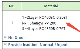
Figure 1: The stackup material parameter
We confirmed the final build and adjusted core/prepreg thicknesses for balance while staying within tolerance. If ignored, the panel could exhibit excessive bow and twist, leading to assembly issues, via cracking during soldering, or even delamination under thermal stress in RF operation. According to IPC-6012 guidelines for multilayer boards, controlling warpage is critical for high-frequency designs where signal integrity depends on consistent dielectric properties.
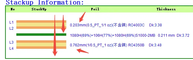
Figure 2: The designed stackup information for controlling warpage
2. Solder Mask Conflict and No-Mask Requirement
The fabrication notes clearly stated “no solder mask,” yet the Gerber files contained full top and bottom solder mask layers that mirrored the copper pattern (with only edge openings differing). This is a classic mismatch we see in RF boards where designers sometimes provide SM data by default.
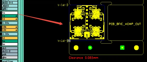
Figure 3: No solder mask on the board
After customer confirmation, we removed all solder mask layers and proceeded with full ENIG on exposed copper. Our CAM team identified this early because proceeding with conflicting data would have resulted in inconsistent surface finish or unwanted mask coverage on RF traces, degrading high-frequency performance. If not clarified, it could cause poor solderability in selective areas or cosmetic defects on the gold surface.
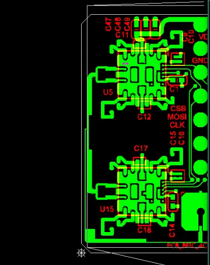
Figure 4: Removed all solder mask layers and proceeded with full ENIG on exposed copper.
3. Blind Via Spacing Violation (0.25 mm Holes)
The 1-2 blind vias were specified at 0.25 mm diameter, but the edge-to-edge spacing between some holes fell below 6 mil. Our engineer noticed this immediately during drill program review: such tight spacing in blind via processing risks drill breakout and unreliable plating.
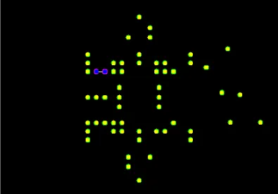
Figure 5: The 1-2 blind vias at 0.25 mm diameter but edge-to-edge spacing between some holes below 6 mil
We recommended and applied copper clearance adjustments around the affected areas. Had this been ignored, production could have seen significant hole breakout, thin or cracked plating, leading to open circuits or high-resistance vias after thermal cycling. In RF applications, this would directly impact signal integrity and reliability. We applied resin plugging + plating fill as required for all 0.25 mm and 0.30 mm holes to ensure flatness and reliability.
4. V-CUT Clearance and Edge Copper Protection
The design required V-CUT on board edges, but copper pours and annular rings were positioned too close to the outline. We noticed that standard V-CUT processing would expose copper on the cut edges.
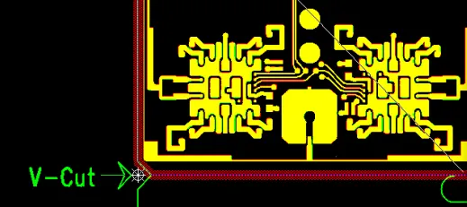
Figure 6: Required V-CUT on board edges
Our team adjusted by cutting back copper 0.35 mm per side along the V-CUT lines. If not addressed, depanelization would leave exposed copper, risking edge shorting during assembly or handling, and potential corrosion over time. Based on IPC-A-600 acceptability criteria, exposed copper near mechanical edges increases defect risk in field use.
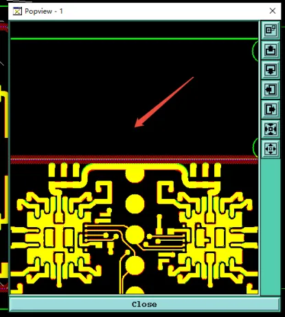
Figure 7: Diagram after cutting back copper 0.35 mm per side along the V-CUT lines
5. Trace/PAD Spacing and Isolated Features
Several areas showed insufficient clearance between traces and pads. We performed targeted copper etching compensation to guarantee safe spacing. Additionally, small isolated copper dots were removed as they increase etching difficulty and risk of copper residue or shorts.
Our CAM engineer confirmed these adjustments because, in 0.5 oz copper processing combined with ENIG, such features can cause yield loss. Ignoring them could result in short circuits or etching defects, especially critical in high-frequency boards where impedance control is essential.
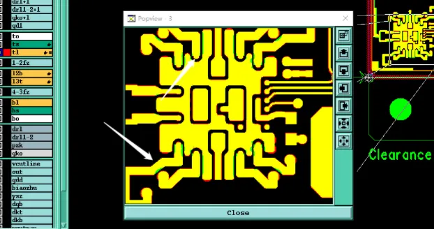
Figure 8: Adjustment because of insufficient clearance between traces and pads
Other Process Clarifications
- We added process edge copper for current balancing during plating.
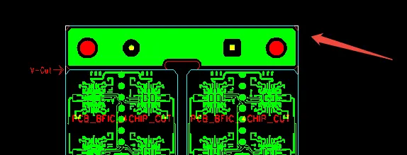
Figure 9: edge copper for current balancing
- Silkscreen characters and frames were added per customer reference images to avoid overlapping pads.
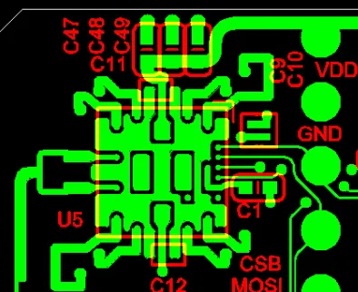
Figure 10: Silkscreen characters and frames on the pad
- Protection rings were added around make points on the top layer after removing process edge copper to prevent detachment.
- Thermal conductivity note (1.0 W/m·K) was noted but followed the specified Rogers materials.
- Gold finger bevel requirement was ignored as no fingers existed on the board.
Manufacturing Risks and DFM Insights
This case highlights several recurring issues in RF PCB design. Hybrid stackups with differing dielectrics require careful symmetry analysis to minimize warpage. Blind via dense arrays must respect minimum spacing for reliable drilling and plating. Fabrication notes must precisely match Gerber data — especially for solder mask on RF boards.
V-CUT designs need explicit clearance considerations, and small features like isolated copper dots often trigger DFM corrections. If these EQs had been ignored, the production run could have suffered 20-30% yield loss from warpage, breakout, or shorts, plus additional delays from rework or scrap boards.
How the Engineering Team Resolved the Issues
We compiled all findings into clear EQ communications with annotated screenshots. After customer confirmation on no solder mask, stackup details, and character placement, we updated the production files accordingly. Our team optimized panelization, applied necessary copper pullbacks, and prepared resin-plugged blind vias with full plating.
Final production data was re-verified, including 100% netlist comparison and impedance considerations for the high-frequency material. The board was released for fabrication only after full alignment with customer intent.
Final Manufacturing Outcome
All engineering questions were resolved through iterative confirmation. Production files were updated with optimized clearances, stackup balance, and process adjustments. The order proceeded to fabrication with reduced risk and improved manufacturability.
Key Takeaways for PCB Designers
- Provide explicit stackup drawings with material types, thicknesses, and symmetry considerations, especially for hybrid Rogers builds.
- Ensure fabrication notes exactly match Gerber content regarding solder mask, silkscreen, and special processes.
- Maintain adequate spacing for blind vias (typically >6-8 mil edge-to-edge depending on diameter) to prevent breakout.
- Design V-CUT and scoring areas with sufficient copper pullback from the mechanical lines.
- Define hole attributes clearly (plated, resin-plugged, etc.) and avoid overly dense via patterns without consultation.
- Remove or flag isolated copper features in layout to improve etching yield.
- Communicate special requirements like no solder mask or characters on gold early in the design phase.
- Perform a thorough DFM check or request factory pre-review for complex RF boards before final Gerber release.
FAQ
Q1: Why is asymmetric hybrid stackup a concern in Rogers PCBs?
A1: Different dielectric constants and thermal expansion rates between RO4003C and RO4350B, combined with unequal thicknesses, can cause warpage during lamination and reflow. This affects assembly flatness and long-term reliability.
Q2: What happens if blind via spacing is too tight?
A2: Drill bits can cause breakout on adjacent holes, leading to incomplete plating, open vias, or weakened mechanical strength. In production this often results in low yield and signal integrity problems.
Q3: Why do factories modify copper near V-CUT lines?
A3: To prevent exposed copper after depanelization, which can cause shorts, corrosion, or assembly defects. Standard practice is to pull back copper by 0.3–0.5 mm depending on process.
Q4: Can RF PCBs be produced without solder mask?
A4: Yes, especially for high-frequency applications where mask can introduce dielectric variation. However, this requires full ENIG coverage and careful handling to avoid oxidation and assembly challenges.
Q5: What is the purpose of resin plugging + plating for blind vias?
A5: It ensures a flat surface for component mounting, improves thermal/electrical performance, and prevents solder wicking or voids in subsequent processes.
Q6: Why remove isolated copper dots during CAM?
A6: Small isolated features are prone to over-etching, incomplete removal, or causing shorts/residues, reducing overall yield in fine-line etching processes.