In March 2026, we reviewed an 8-layer HDI PCB order sized 88.4 × 90.2 mm with 1.0 mm finished thickness. The design featured blind vias, resin-plugged vias, customer panelization (2×2), and TG170 FR-4 material. Although a standard medium-volume order, the CAM engineering review uncovered several critical manufacturability issues involving inner layer copper distribution, BGA pad design, blind via processing, and panelization details.
HDI boards with blind vias and dense BGA areas are highly sensitive to DFM details. Our team identified multiple risks that could lead to lamination failure, assembly defects, or reliability issues if not addressed before production.
Order Overview
This was an 8-layer FR-4 TG170 PCB ( #FR4-20260505-010 ) with 1 oz copper on inner and outer layers, 1.0 mm thickness, and ENIG surface finish (2U"). Minimum hole size was 0.3 mm, with blind vias implemented. The board used customer self-panelization in 2×2 format with V-CUT + routing separation. Order quantity was 400 pcs (100 sets). 100% flying probe testing was required. Special processes included resin plugging and blind via laser drilling.
Main Engineering Questions Found During CAM Review
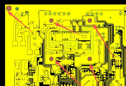
1. Low Copper Density on Inner Layers (L3 & L6) – Lamination Risk
Our CAM engineer identified that L3 and L6 layers had only routing and isolated pads with almost no copper pour. We noticed this extremely low copper density would cause severe resin flow imbalance during lamination.
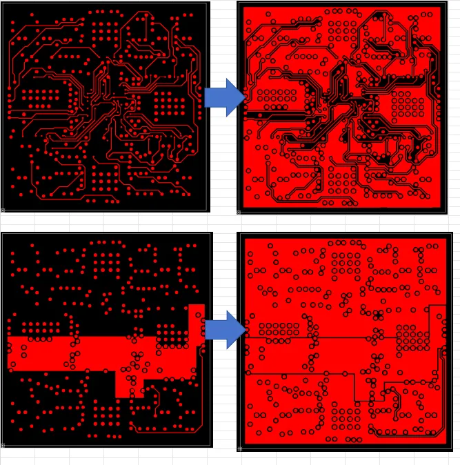
Figure 1: L3 and L6 layers had almost no copper pour
To reduce risk, we recommended adding production copper balancing while preserving electrical performance. We sent the proposed modification for customer confirmation.
If this issue had been ignored, the board would likely suffer delamination, resin voids, or board explosion during pressing. We have seen similar low-copper inner layers cause complete panel scrap in multi-layer builds.
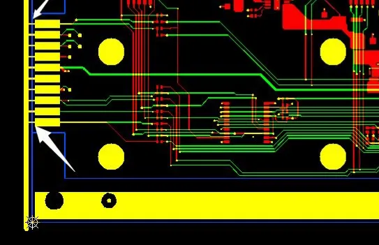
2. NSMD BGA Pads and Silkscreen Frame Concerns
The Gerber data used Non-Solder Mask Defined (NSMD) pads in the BGA area. Additionally, the silkscreen character frame around BGA was too high, which could cause component floating and cold solder joints during assembly.
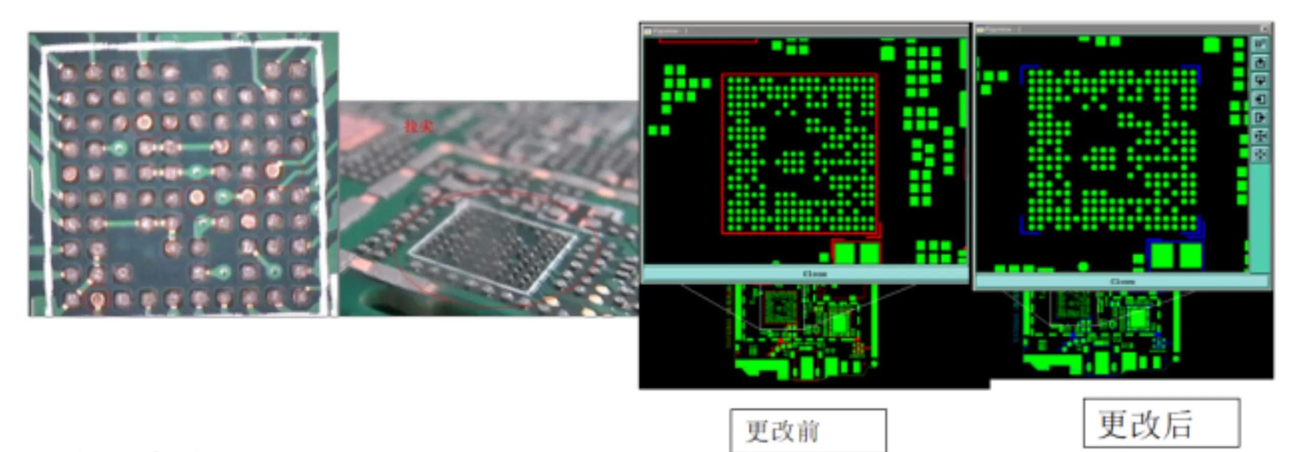
Figure 2: before and after reducing or removing the silkscreen frame in BGA regions
We recommended reducing or removing the silkscreen frame in BGA regions to improve solderability and suggested careful evaluation of NSMD pads to prevent pad cratering. The customer was asked to confirm modifications.
Without adjustment, NSMD pads increase the risk of pad lift (cratering) under thermal stress, while high silkscreen frames often lead to assembly defects and field failures.
3. Blind Via Solder Mask Openings and Laser Drill Size
Multiple blind vias (including 0.127 mm laser vias on layers 1-2, 1-3, 1-4) had solder mask openings on pads. This is non-standard for HDI designs. We also confirmed the small laser drill diameter suitability for our process.
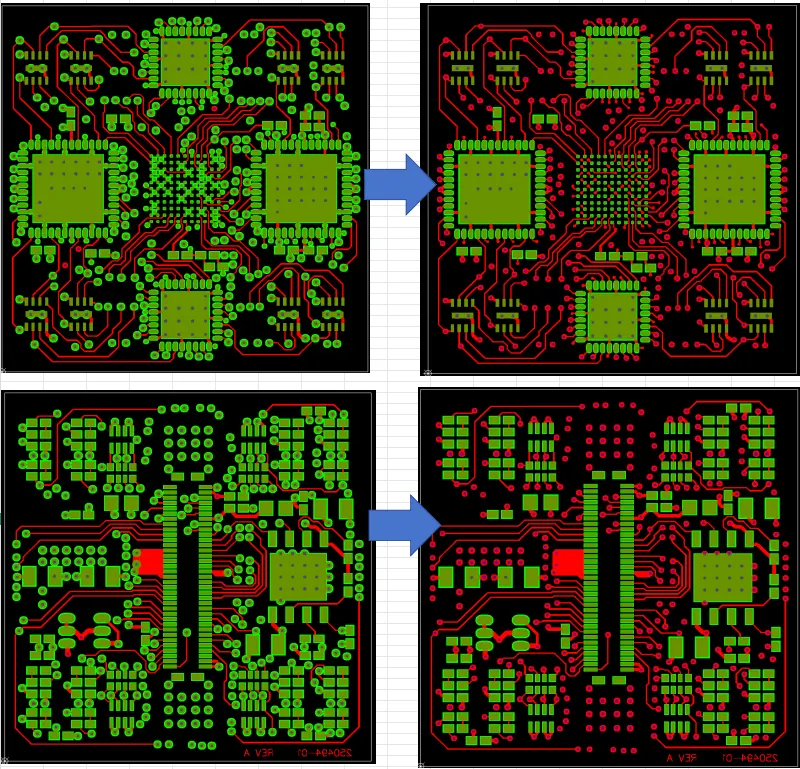
Figure 3: blind vias had solder mask openings on pads
We raised clarification on whether these openings were intentional or should be tented to improve reliability.
4. Panelization, V-CUT and Process Edge Issues
The panel included both V-CUT and stamp holes, which could weaken bridges. Process edges had sharp corners that risk damaging dry film and packaging. We also clarified version consistency across layers and files, and proposed a stackup using standard FR-4 TG170 material.
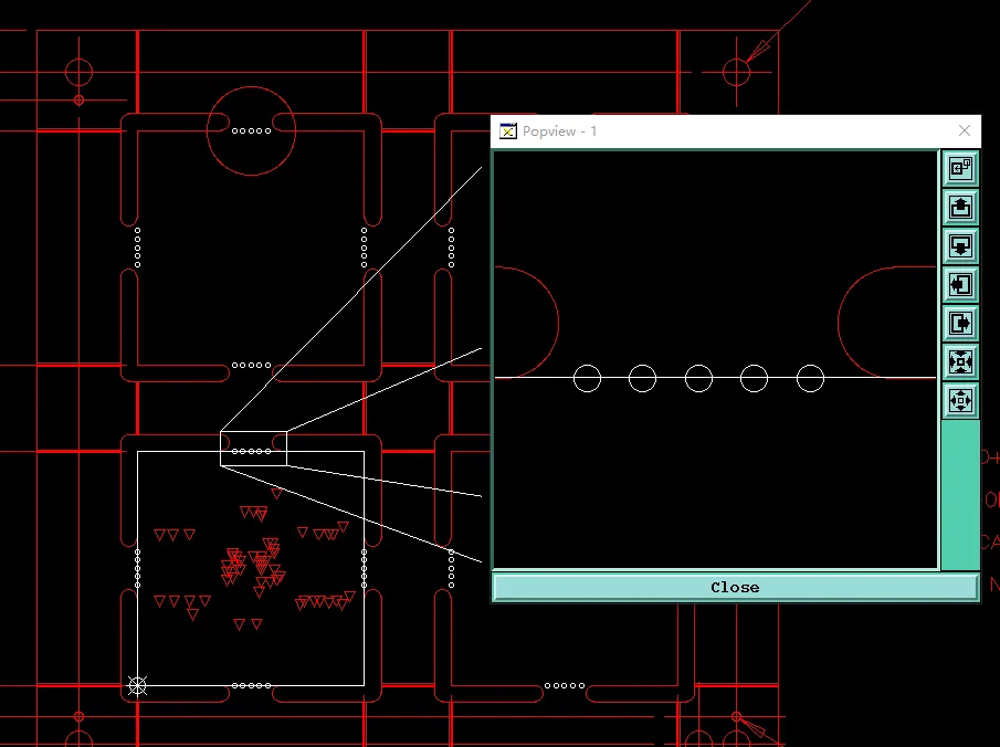
Figure 4: panel included both V-CUT and stamp holes
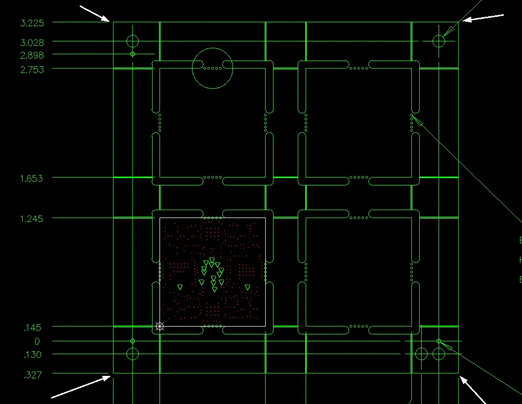
Figure 5: Process edges had sharp corners
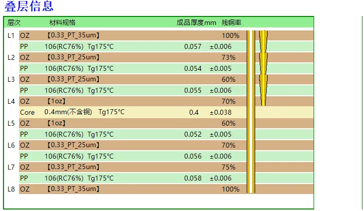
Figure 6: standard FR-4 TG170 material stackup
Manufacturing Risks and DFM Insights
This case illustrates common HDI pitfalls: unbalanced copper distribution on inner layers is one of the top causes of lamination failure in 8+ layer boards. NSMD BGA pads combined with high silkscreen frames frequently cause assembly yield loss. Small laser blind vias with mask openings add unnecessary risk of exposed copper and reliability concerns.
Combining V-CUT with stamp holes and using sharp process edges are frequent sources of handling damage and broken panels during transport.
How the Engineering Team Resolved the Issues
Our engineering team prepared detailed annotated files and a recommended stackup. We suggested copper balancing on L3/L6, silkscreen adjustments in BGA areas, and clarification on blind via mask strategy. After customer feedback, production files were updated with optimized panelization, consistent versioning, and safer process edge design.
To reduce manufacturing risk, we adjusted V-CUT parameters and confirmed material stackup for reliable lamination.
Final Manufacturing Outcome
All engineering questions were clarified and approved. Production data was finalized with balanced copper, optimized mask design, and safe panelization. The order successfully passed DFM review and was released for fabrication.
Key Takeaways for PCB Designers
- Avoid extremely low copper density on inner layers — add balanced copper pour where possible to prevent delamination.
- Use SMD-defined pads for BGA areas when possible to reduce cratering risk; minimize silkscreen in BGA regions.
- Be cautious with solder mask openings on blind via pads in HDI designs.
- Provide consistent version information across all layers, files, and documentation.
- For V-CUT panels, avoid combining with stamp holes in the same area to maintain connection strength.
- Design process edges with rounded corners to prevent damage to dry film and packaging.
- Always confirm laser drill sizes and stackup early for HDI projects with blind vias.
FAQ
Q1: Why is low copper density on inner layers a problem?
A1: It causes uneven resin flow and pressure during lamination, leading to delamination, voids, or board explosion.
Q2: What are the risks of NSMD BGA pads?
A2: Reduced mask support increases the chance of pad cratering (lift-off) during thermal cycling or assembly stress.
Q3: Should blind vias have solder mask openings?
A3: Usually not recommended in HDI designs. Openings can expose copper after plating and reduce reliability.
Q4: Can V-CUT and stamp holes be used together?
A4: It is possible but weakens the panel bridges. This combination increases the risk of premature breaking during handling and transport.
Q5: Why confirm stackup even with standard material?
A5: Different material variants have varying Dk and resin content. Confirmation ensures proper impedance (if needed) and lamination quality.