In daily CAM engineering work, 8-layer boards with mixed copper weights and blind or buried vias frequently require detailed engineering questions during DFM review. This case study covers order a compact 77.5 x 60 mm 8-layer FR-4 TG170 board. During our standard engineering review, several critical manufacturability issues were identified that needed multiple rounds of customer clarification before safe release to production.
Our CAM team found inconsistencies between the ordered parameters, Gerber data, provided lamination structure, and actual manufacturing requirements. These issues highlight the common gap between design intent and fabrication capability. Below is a detailed engineering analysis of what we discovered and how the issues were resolved.
8-Layer 1.6mm FR-4 TG170 PCB Order Specifications and Via Requirements
This was an 8-layer rigid PCB ( #FR4-20260115-006 ) built on FR-4 TG170 material with 1.6 mm finished thickness. Outer layers were specified as 1 oz copper and inner layers as 0.5 oz. The design used ENIG surface finish, 0.1 mm minimum hole size, 5 mil trace and space, and 100% flying probe testing. Panelization was 1x1 with routing plus V-scoring separation. The order quantity was 10 pieces. The board included blind and buried vias, with mechanical forming and aluminum foil plugged vias.
Although the parameters appeared standard, the combination of mixed copper weights, buried vias spanning layers 2-7, and discrepancies in the lamination structure created several production risks that required immediate clarification.
Critical DFM Issues Identified in 8-Layer TG170 PCB CAM Review
1. Copper Weight Mismatch in Lamination Structure and Order Parameters
Our engineer first identified a clear conflict in copper thickness. The customer ordered inner layers 0.5 oz and outer layers 1 oz, but the provided lamination structure indicated L2 and L7 as 1 oz while L3 to L6 were 0.5 oz. This mismatch affects etch compensation, potential impedance control, and finished board thickness calculation.
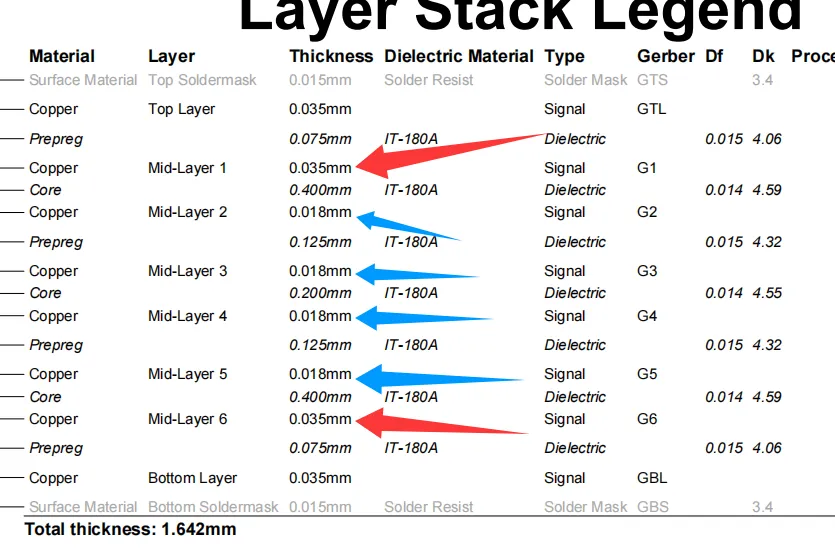
Figure 1: lamination structure indicated L2 and L7 as 1 oz while L3 to L6 were 0.5 oz
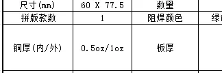
Figure 2: inner layers 0.5 oz and outer layers 1 oz
We noticed this discrepancy early during stackup verification. After clarification with the customer, we adjusted the working files and stackup to ensure consistency with the ordered copper weights.
If left unaddressed, mismatched copper weights could result in incorrect etch factors, leading to trace width deviations beyond IPC-6012 tolerances, potential open circuits on fine features, or impedance variations that surface only after assembly.
| Layer | Ordered | Structure Indicated |
|---|---|---|
| Outer Layers | 1 oz | 1 oz |
| Inner Layers | 0.5 oz | Mixed (L2/L7 1 oz) |
Table 1: Copper Weight Specification vs Lamination Structure
2. Buried Via (Layers 2-7) Plating Feasibility and Stackup Optimization
This was the most critical issue in the review. The customer's reference lamination structure required buried vias between layers 2 and 7. However, with the planned build-up, proper copper plating for these buried vias would be impossible without violating the ordered copper weights or requiring additional complex plating steps.
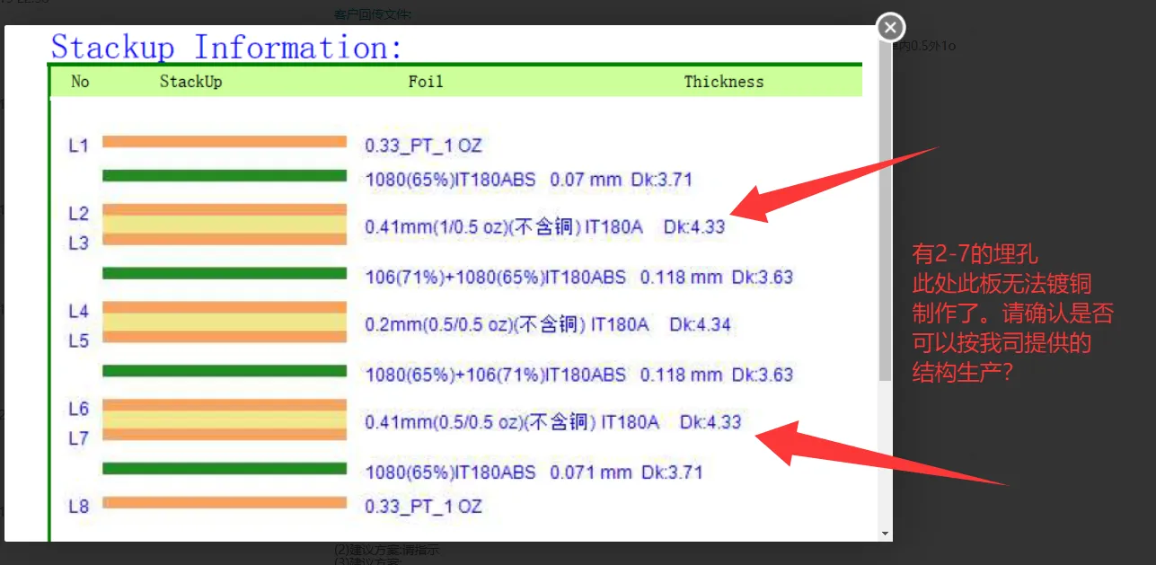
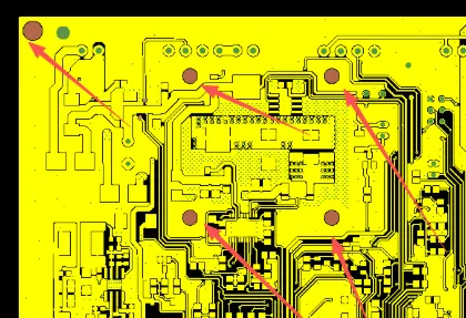
Figure 3: lamination structure required buried vias between layers 2 and 7
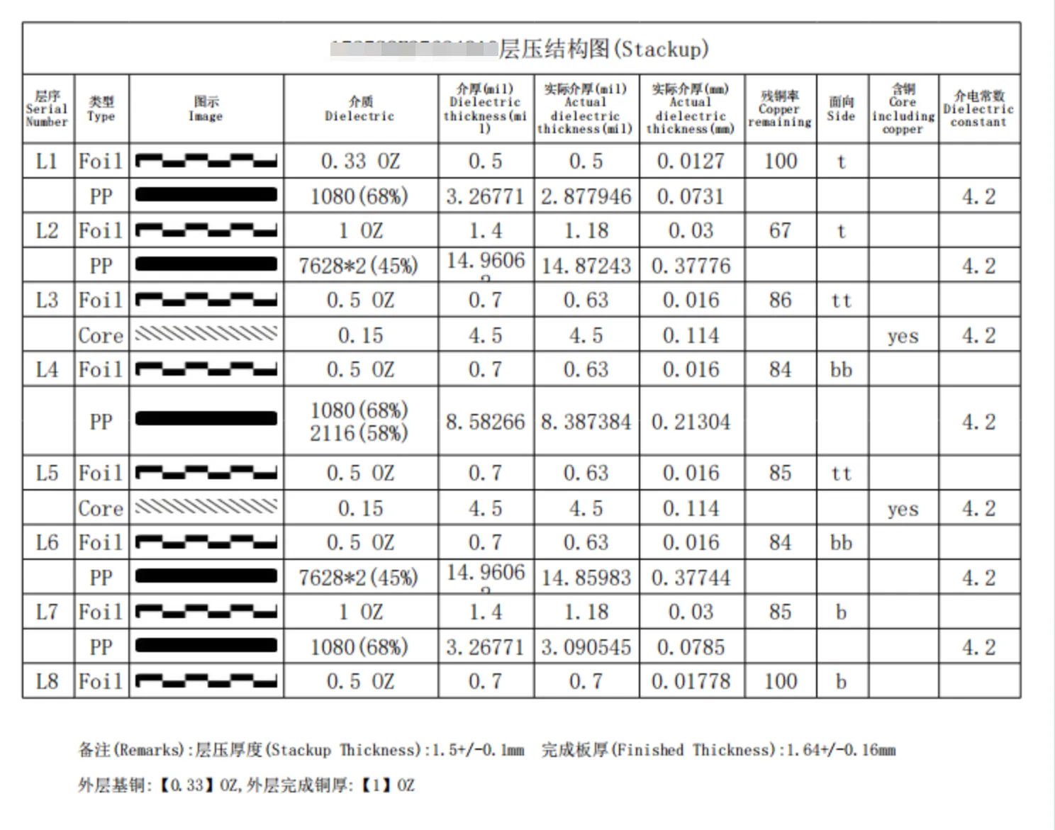
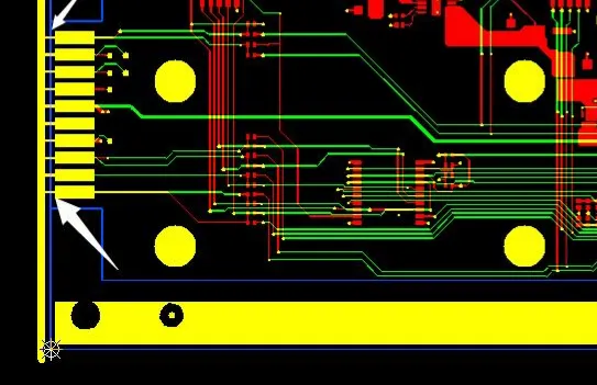
Figure 4: PCB stackup thickness
Our CAM team identified this during detailed lamination analysis. We recommended adjustments to the stackup and provided optimized working files for customer approval. We confirmed that the original structure could not support reliable plating for the specified buried vias.
If ignored, the buried vias would suffer from insufficient plating thickness. This commonly leads to via cracking under thermal stress, open circuits after reflow, or early field failures. According to IPC-TM-650 requirements for plated structures, adequate copper wall thickness must be achieved regardless of via span.
We optimized the lamination sequence and working gerber to ensure all buried vias could be properly drilled, desmeared, and plated while staying within the customer's copper weight constraints.
3. Finished Board Thickness Tolerance and Stackup Verification
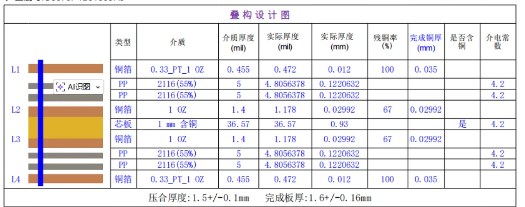
The customer-provided lamination structure calculated to approximately 1.642 mm finished thickness, while the order specified 1.6 mm. We raised this for confirmation to determine whether 1.6 mm or 1.64 mm +/-10% should be controlled.
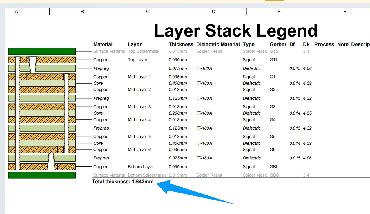
Figure 5: PCB with 1.642 mm finished thickness
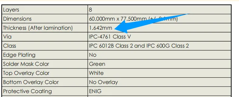
Figure 6: table shows a PCB with 1.642 mm finished thickness
Board thickness tolerance is critical for mechanical fit in final assemblies. Deviation beyond expected limits can cause issues with enclosure fit or increased mechanical stress on components.
4. Solder Mask and Paste Layer Consistency with Exposed Copper Areas
We identified mismatches between solder mask openings and the solder paste layer. Specific areas required confirmation on whether additional openings should be added to the paste data. We also clarified regions where exposed copper was acceptable versus areas requiring full solder mask coverage, including etch line frames.
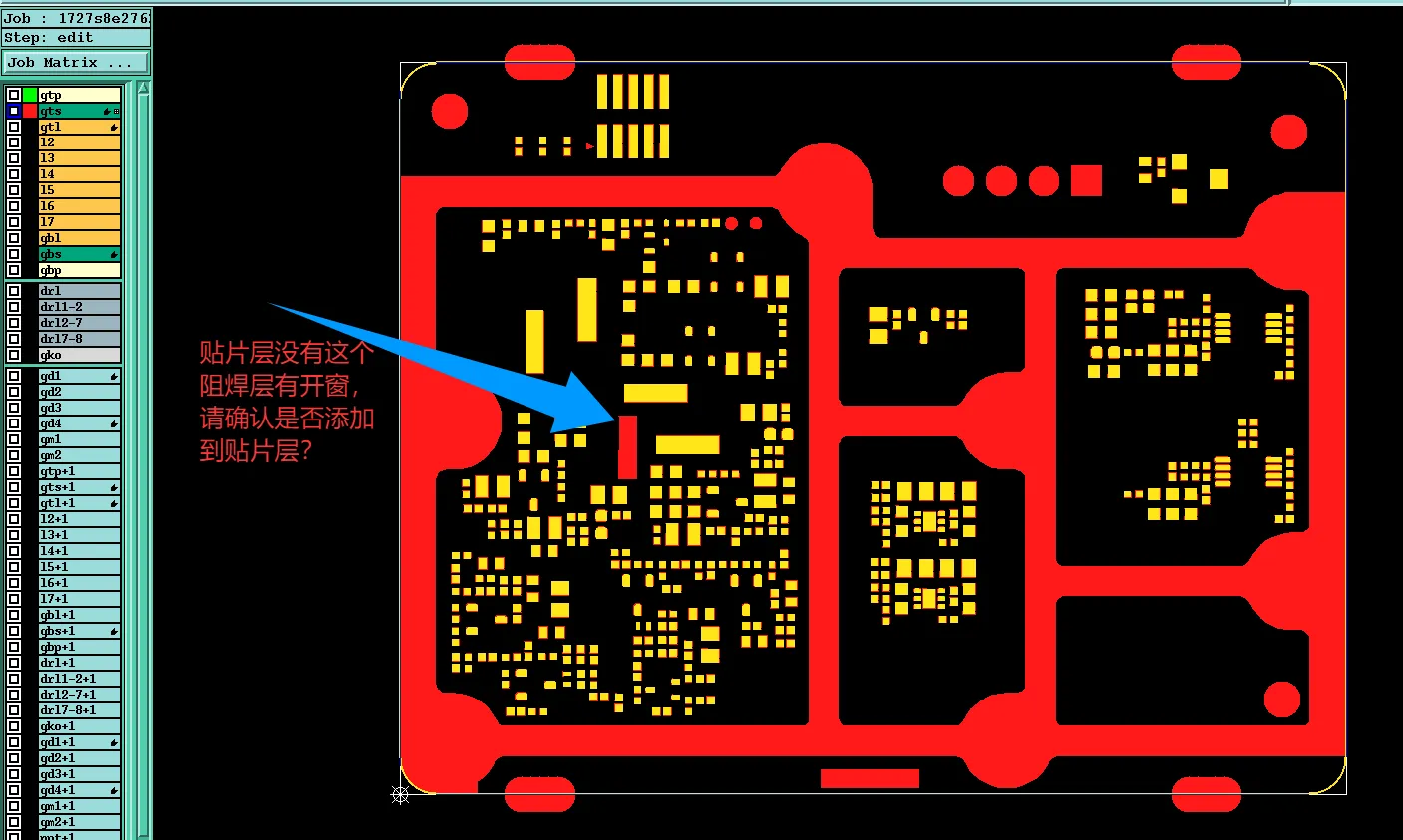
Figure 7: mismatches between solder mask openings and the solder paste layer
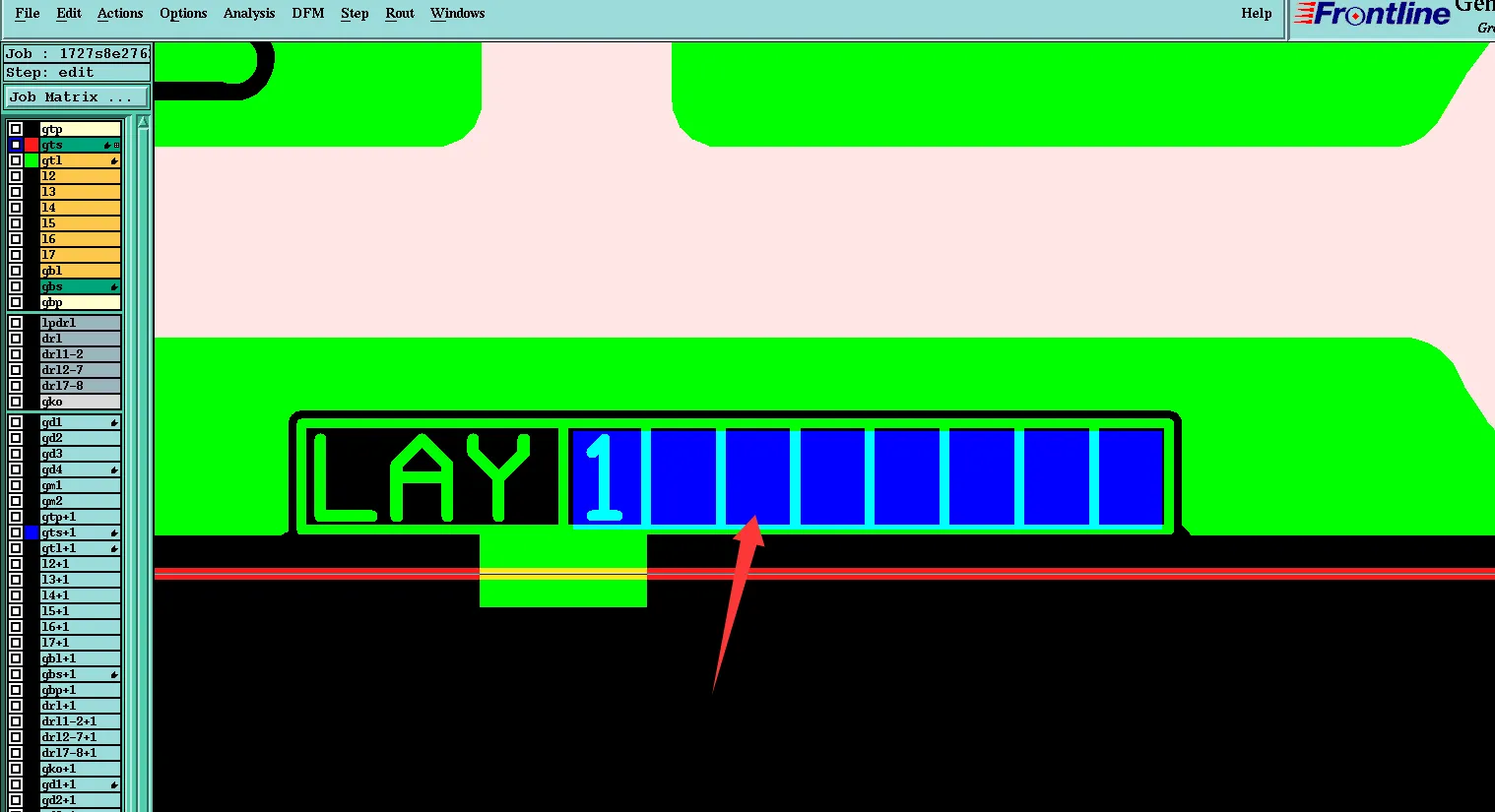
Figure 8: the etched line frame has an ink cover and opening
Our engineer noted that inconsistent solder mask and paste data can lead to solder bridging, insufficient paste volume, or poor solder joint reliability during SMT assembly.
No silkscreen layer was present in the provided Gerber files. We confirmed production with green solder mask and no legend marking.
5. File and Marking Issues
The customer-provided DOB data could not be opened, so production proceeded based on Gerber files after confirmation. We also handled requests for adding specific regulatory markings (such as UL) on the bottom solder mask layer, referencing patterns from similar previous orders.
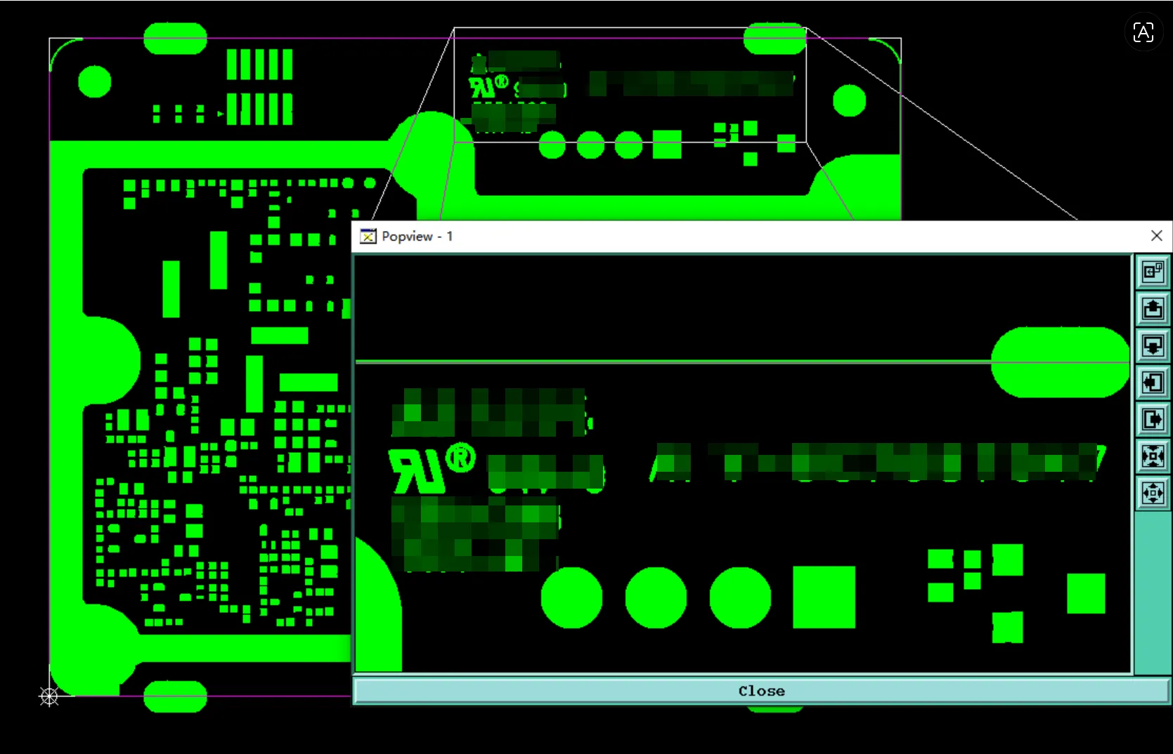
Figure 9: UL markings
Key Manufacturing Risks in 8-Layer TG170 PCB with Buried Vias
This case demonstrates common DFM challenges in multilayer designs involving buried vias and mixed copper weights. Designers frequently define stackups without fully accounting for sequential lamination and plating process limitations. When buried vias span layers that become problematic in the final build-up, plating reliability is compromised.
Unresolved copper weight conflicts often cause etching inconsistencies, trace width errors, and potential shorts or opens on fine features. The buried via plating issue carried the highest reliability risk - inadequate plating frequently results in via failures during thermal cycling or in-field operation.
These types of issues, if ignored, lead to production delays, increased scrap rates, and potential costly field returns.
Collaborative EQ Resolution and Optimized Stackup for TG170 Board
Our team maintained clear iterative communication, providing updated working files and annotated stackup drawings at each step. We optimized the lamination structure to meet both electrical requirements and manufacturing constraints while adhering to the ordered copper weights. After final customer approvals on stackup, via feasibility, solder mask details, and thickness tolerance, all engineering questions were resolved.
Successful Production Release After Full Stackup and Via Alignment
All engineering clarifications were completed successfully. The stackup was optimized, copper weights aligned, buried via plating confirmed feasible, and documentation details approved. The order was released for production with updated fabrication parameters.
Essential DFM Guidelines for 8-Layer TG170 PCB with Complex Vias
- Provide a clear layer-by-layer stackup diagram showing actual copper weights and dielectric thicknesses that exactly match your order specifications.
- Verify buried and blind via spans against the intended lamination sequence early in the design process.
- Ensure solder mask and solder paste layer data are fully consistent to prevent SMT issues.
- Confirm finished board thickness tolerance and provide stackup calculations that align with ordered values.
- Include all special fabrication requirements directly in Gerber layers or a clear accompanying document.
- Explicitly confirm the absence of silkscreen when no legend layer is provided.
- Supply vector data for any required markings such as UL or company logos.
- Engage with your manufacturer early when using complex via structures or mixed copper weights.
| Area | Recommendation |
|---|---|
| Stackup | Provide clear layer-by-layer diagram |
| Buried Vias | Align span with lamination sequence |
| Markings | Define content and location clearly |
Table 2: 8-Layer TG170 PCB DFM Recommendations
FAQ
Q1: Why is buried via span critical in multilayer stackup design?
A1: Buried vias must be drilled and plated at specific stages of the lamination process. If the via connects layers that end up near the surface in the final build, achieving reliable plating thickness becomes difficult, increasing the risk of via cracking and reliability failures.
Q2: What problems can occur from copper weight mismatches in the stackup?
A2: Different copper thicknesses require different etch compensation. Mismatches can cause trace width errors, impedance deviations, and potential shorts or opens, especially on fine-line designs.
Q3: Why do factories compare solder mask openings with the paste layer?
A3: Solder mask defines exposed copper areas while paste defines solder deposition volume. Inconsistencies can lead to insufficient solder, bridging, or poor joint reliability during assembly.
Q4: How important is finished board thickness tolerance?
A4: Very important for mechanical assembly. Deviations can prevent proper fitting into enclosures or cause stress on connectors and components.
Q5: Should designers always provide a detailed fabrication drawing?
A5: Yes, especially when special requirements such as exposed copper areas, specific tolerances, or markings are needed. Clear documentation significantly reduces engineering questions and manufacturing risks.
Q6: What is the risk of proceeding without resolving stackup and via issues?
A6: High risk of scrap boards, production delays, unreliable interconnections, and potential field failures. Early resolution protects both delivery schedule and product reliability.