In February 2026, we processed a 4-layer heavy copper PCB order with 3oz copper on both inner and outer layers. Although only 4 layers, the combination of 1.2mm thickness, heavy copper, V-CUT + routing panelization, plated milling slots, and resin-plugged vias created several manufacturability challenges during CAM review.
Heavy copper boards with mechanical scoring and edge-proximate components frequently require engineering clarification. Our CAM team identified multiple critical issues that, if left unaddressed, could lead to pad damage, incorrect slot plating, or lamination inconsistencies. This case demonstrates why even seemingly straightforward 4-layer jobs demand thorough DFM validation before production release.
Order Overview
This was a 4-layer FR-4 TG150 PCB ( #FR4-20260427-053 ) measuring 96.1 × 187 mm with 1.2 mm finished thickness and 3oz copper weight on all layers. The board used ENIG surface finish, 0.3 mm minimum hole size, and no impedance control. Panelization was customer self-panel 1×4 with V-CUT + routing separation. Order quantity was 500 pcs (125 sets). Special processes included resin plugging, plated milling slots, and microsection requirements. 100% flying probe testing was specified.
Fabrication notes mentioned milling by MILLING.gbr, plated milling by PLATED_MILLING.gbr, and V-scoring by V-CUT.gbr, highlighting the importance of precise mechanical feature definition.
Main Engineering Questions Found During CAM Review
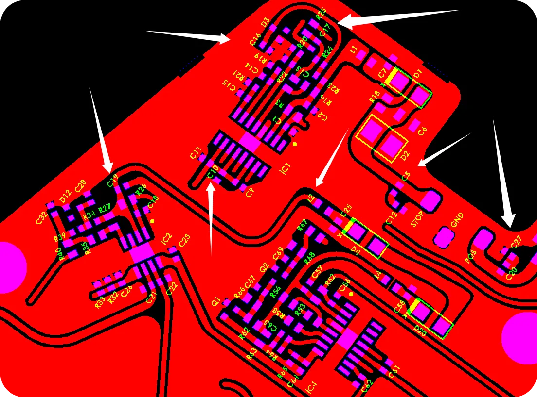
1. SMD Pads Too Close to V-CUT Line – Risk of Copper Damage
We noticed several SMT pads positioned extremely close to the V-CUT line. After simulating the scoring process, our engineer determined that depanelization would cut into portions of these pads.
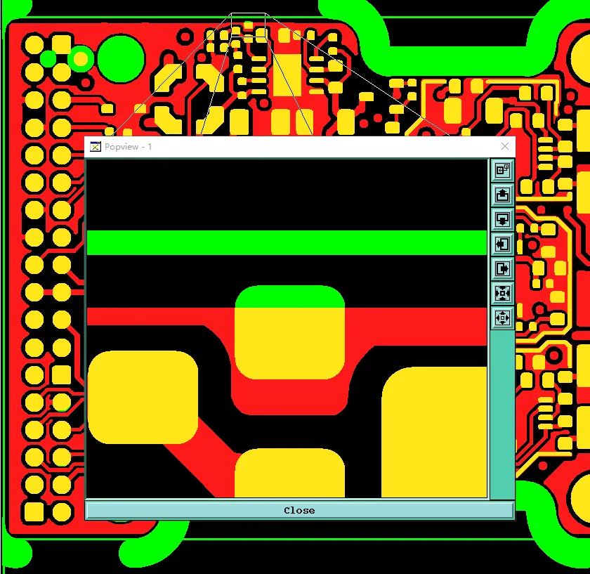
Figure 1: SMT pads positioned extremely close to the V-CUT line
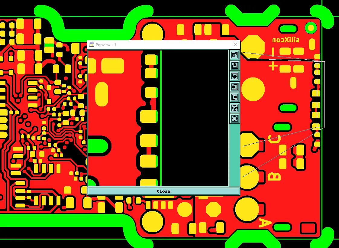
Figure 2: SMT pads positioned extremely close to the V-CUT line
This is a common issue in dense panel layouts with heavy copper. We immediately raised an EQ with annotated images showing the overlap and asked for customer confirmation on whether to move the pads, adjust V-CUT position, or accept partial pad removal.
If ignored, V-CUT would have severed pad edges, leading to exposed copper on the board edge, poor solderability, and potential assembly shorts or cosmetic rejects. In heavy copper boards, such damage is difficult to repair and often results in high scrap rates after assembly.
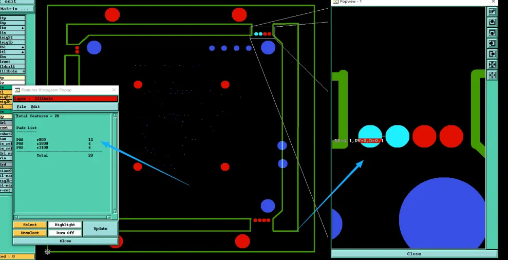
2. Plated vs Non-Plated Slots Clarification
The fabrication notes called for plated milling on specific slots. However, four slots appeared ambiguous in the latest data. Our CAM team compared with previous revisions and confirmed the requirement for copper-plated slots using the PLATED_MILLING.gbr layer.
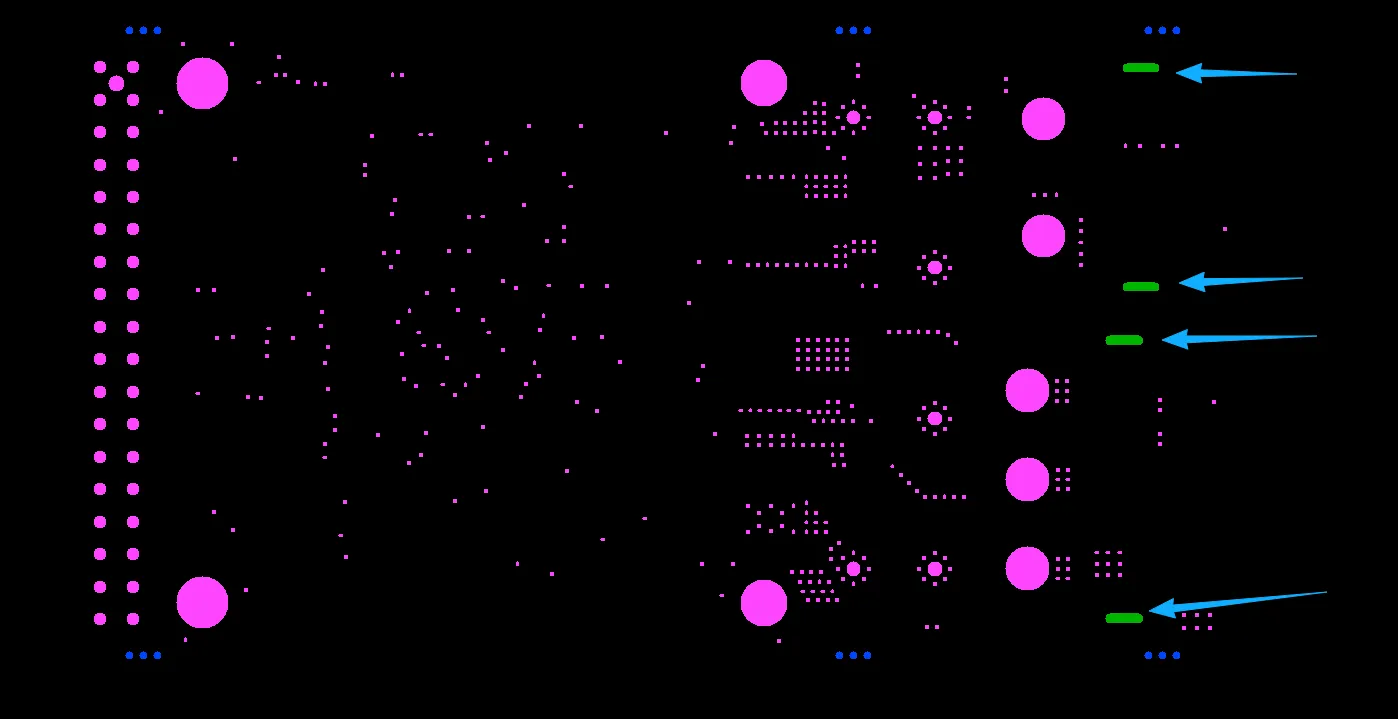
Figure 3: four slots appeared ambiguous in the latest data
We asked the customer to verify whether these four slots should be plated (with copper) or non-plated. Incorrect plating decision would either leave functional slots without conductivity or add unnecessary copper where isolation was intended.
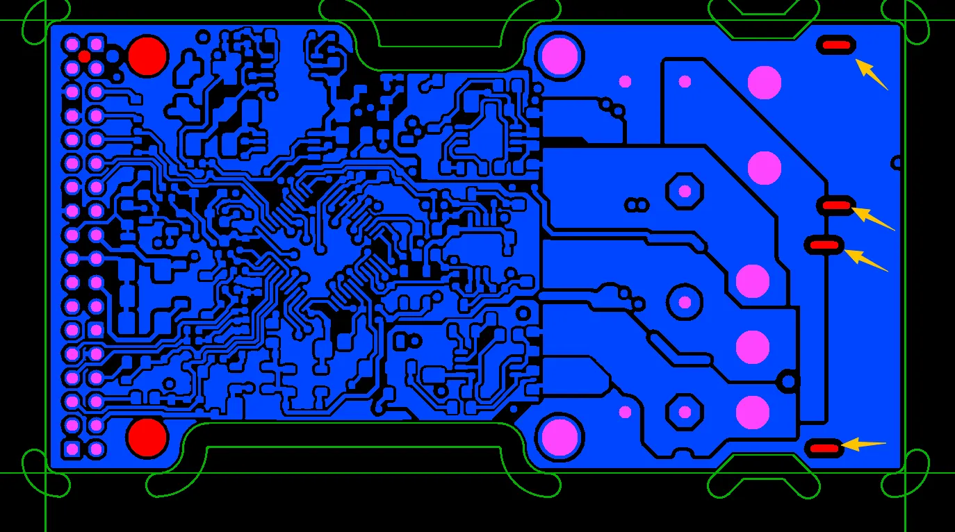
Figure 4: these four slots should be plated (with copper) or non-plated
Proceeding without confirmation risked functional failure — plated slots where isolation was needed could cause short circuits, while non-plated where connectivity was required would result in open circuits.
3. Stackup Confirmation Using Factory Standard Materials
The customer did not provide a custom stackup. We prepared one based on our standard TG150 FR-4 material library suitable for 3oz heavy copper and 1.2mm thickness. Our engineering team sent the detailed press stack for confirmation.
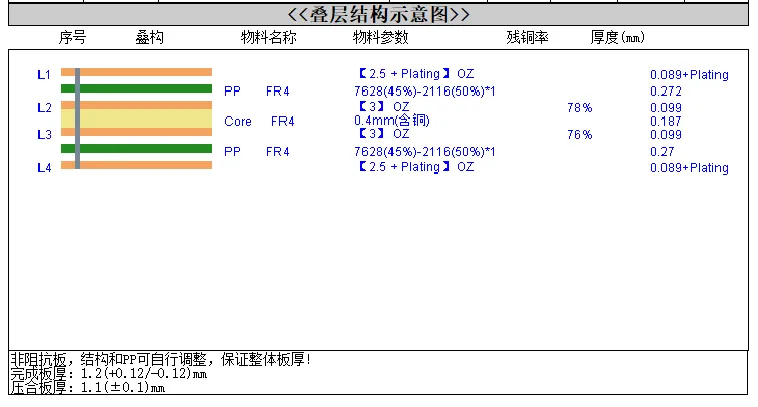
Figure 5: our standard TG150 FR-4 material library
For heavy copper boards, dielectric thickness and resin content directly affect registration and copper adhesion. We needed explicit approval before lamination.
4. Inner Layer Copper Connectivity (L3) and Resin Plugging Questions
Netlist check on L3 revealed two copper areas that were not electrically connected. We asked whether they should be joined. Additionally, for resin-plugged vias, we confirmed whether the blue vent holes (air-release holes) also required plugging.
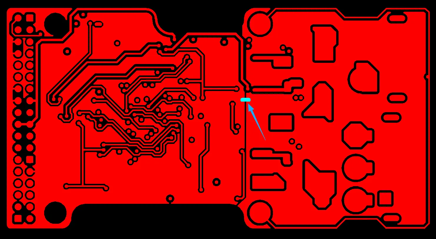
Figure 6: two copper areas that were not electrically connected
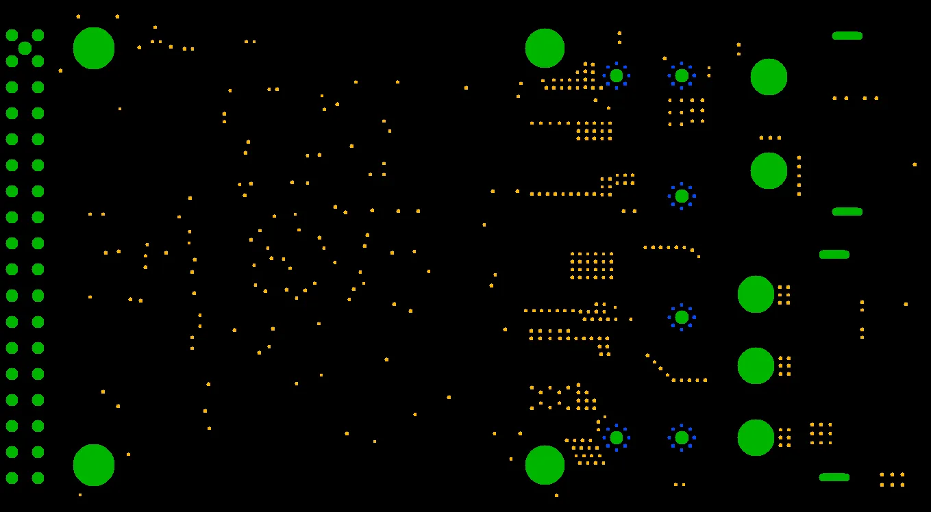
Figure 7: the blue vent holes (air-release holes) also required plugging
We also clarified solder mask opening strategy: plugin holes to follow trace pads, other pads enlarged by 1mil to account for ink flowback, and addition of production cycle codes on top solder mask.
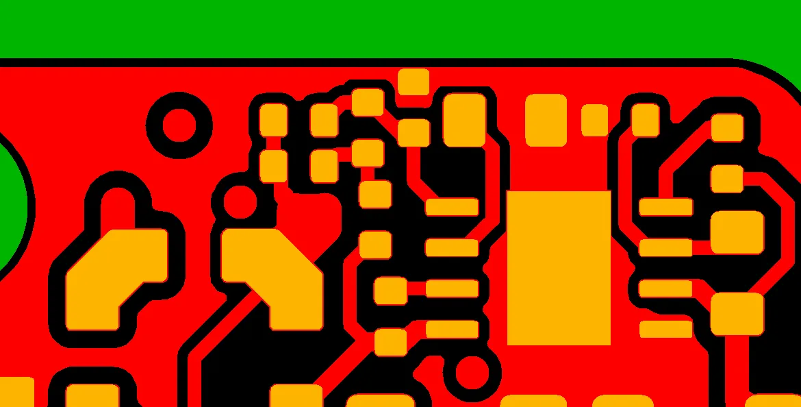
Figure 8: solder mask opening strategy
Figure 9: addition of production cycle codes on top solder mask
Unconnected copper on inner layers could cause unexpected signal behavior, while incorrect via plugging would affect reliability and planarity.
Manufacturing Risks and DFM Insights
This case highlights typical pitfalls in heavy copper designs with mechanical depanelization. Placing components too close to V-CUT lines is one of the most frequent causes of post-assembly defects in scored panels. Heavy 3oz copper exacerbates the issue because the thicker metal is harder to cut cleanly and more prone to burrs and edge delamination.
Ambiguous slot plating definitions and missing features between revisions also commonly trigger multiple data exchange cycles, delaying production. For resin plugging, distinguishing functional vias from vent holes is critical to avoid trapped air or uneven surface finish.
How the Engineering Team Resolved the Issues
Our CAM engineer prepared clear annotated screenshots and revised production files showing proposed V-CUT adjustments and slot definitions. After customer confirmation on pad positions, plated slots, stackup, and plugging requirements, we updated all mechanical layers and added the production cycle marking on the solder mask.
To reduce risk, we adjusted the panelization data to better protect edge pads while maintaining customer panel dimensions. All clarifications were documented and incorporated into the final manufacturing package.
Final Manufacturing Outcome
Following customer approvals on all engineering questions, the production data was finalized, DFM checks passed, and the order was released for fabrication. The board moved successfully into production with optimized milling, scoring, and plugging parameters.
Key Takeaways for PCB Designers
- Keep SMT pads at least 0.3–0.5 mm away from V-CUT lines depending on copper weight to prevent edge damage during depanelization.
- Clearly specify plated vs non-plated slots in both fabrication notes and dedicated Gerber layers (e.g., PLATED_MILLING.gbr).
- Always provide or approve stackup drawings when using heavy copper, especially for boards requiring microsection analysis.
- Coordinate resin plugging requirements carefully — distinguish between functional vias and vent/air-release holes.
- Maintain version control on mechanical files to avoid missing slots or features between revisions.
- Define solder mask expansion rules explicitly, considering ink flow on heavy copper pads.
- Include production marking requirements (date codes, serials) early to avoid last-minute solder mask revisions.
FAQ
Q1: Why do SMT pads near V-CUT lines often cause problems?
A1: During scoring and breaking, the blade can cut into or lift pad edges, especially on heavy copper. This leads to exposed copper, solderability issues, and potential shorts after assembly.
Q2: What is the difference between plated and non-plated milled slots?
A2: Plated slots have copper walls for electrical connectivity or shielding; non-plated are for mechanical mounting or clearance. Wrong specification causes short or open circuits.
Q3: Should vent holes (air release) be resin plugged?
A3: Usually not. Vent holes are designed to release air during lamination or plugging. Plugging them can trap air or create voids, while leaving functional vias open affects reliability.
Q4: Why do factories ask for stackup confirmation even on standard 4-layer boards?
A4: Heavy copper changes dielectric requirements and affects registration and thickness tolerance. Confirmation ensures the final board meets both mechanical and electrical expectations.
Q5: What happens if inner layer copper islands are left unconnected?
A5: Floating copper can cause etching inconsistencies, potential shorting after assembly, or unexpected antenna effects in high-speed applications.