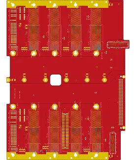
ENIG FR4 PCB Production Record #FR4-20260309-026
| Parameter | Value | Parameter | Value |
|---|---|---|---|
| PCB Type | FR4 PCB | Quantity | 5 pcs |
| Layers | 24 Layers | Board Type | Single PCB |
| Dimensions | 279.7 x 215.57 mm | Copper Weight | 1oz |
| Thickness | 3 mm | Min Track / Spacing | 4/4mil |
| Surface Finish | ENIG (Immersion Gold) | Min Hole Size | 0.4mm |
| Solder Mask | Red | Silkscreen | White |
| Stack-up | Custom | Impedance Control | Yes |
This 24-layer FR4 PCB order consisted of 5 single boards sized 279.7 × 215.57 mm with a finished thickness of 3.0 mm. Using 0.5 oz / 1 oz copper and ENIG surface finish, the design incorporated impedance control and multiple high-precision features including press-fit holes and extensive back-drilling.
During DFM review, several critical issues were identified: press-fit holes had stringent requirements on finished hole diameter, copper wall thickness, nickel and gold plating; back-drilling required a maximum 4 mil stub length and specific depth control in BGA regions, which are difficult to achieve consistently and could lead to signal integrity problems or mechanical failure if out of spec. Additionally, significant copper density difference between top and bottom layers posed warpage risk on the thick board, via resin plugging conflicted with bottom-side solder mask window design, and solder mask bridge dimensions were below standard capability.
Through detailed engineering clarifications and customer confirmations, process parameters were optimized, including adjusted drilling compensation, plating controls, back-drill programs, and selective plugging strategy. The order was successfully completed within the 33-day window with 100% electrical testing, meeting all impedance, thickness, and mechanical requirements.
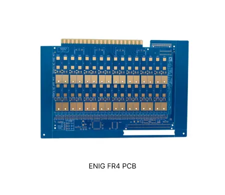
FR4 material with ENIG finish provides balanced electrical performance, shelf life, and assembly compatibility for industrial and high-reliability electronics.
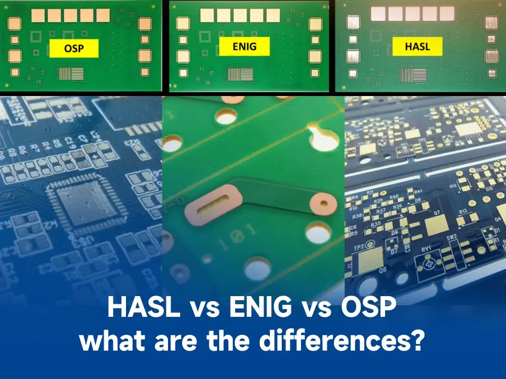
Explore common engineering queries in ENIG, HASL, and OSP FR4 PCBs. Learn real DFM challenges, surface finish compatibility issues, and practical solutions to reduce manufacturing risks and improve yield.
| Order ID | PCB Type | Layers | Dimensions | Solder Mask | Surface Finish | Quantity | Action |
|---|---|---|---|---|---|---|---|
| FR4-20260630-014 | FR4 PCB | 2 | 126 x 145 | Green | ENIG (Immersion Gold) | 10 | View detail |
| FR4-20260529-059 | FR4 PCB | 2 | 147.3 x 53.8 | Green | ENIG (Immersion Gold) | 5 | View detail |
| FR4-20260520-046 | FR4 PCB | 2 | 94.21 x 275 | Green | ENIG (Immersion Gold) | 75 | View detail |


