Introduction
ENIG, HASL, and OSP are the three most common surface finishes for FR4 PCBs. Each has distinct advantages and process requirements, but the choice of finish is also one of the biggest sources of Engineering Queries (EQ) during CAM review and production. In actual order processing, mismatches between the finish selected on the quote page and the specifications in Gerber files frequently cause delays, revisions, and extra communication.
This article consolidates the most frequent real-world EQs for ENIG FR4, HASL FR4, and OSP FR4 PCBs based on factory CAM experience. It highlights key differences, common pitfalls, and actionable design rules to help engineers make the right finish decision and minimize EQs before production begins.
Case 1: Surface Finish Mismatch Between Quote and Gerber Files
Case Overview
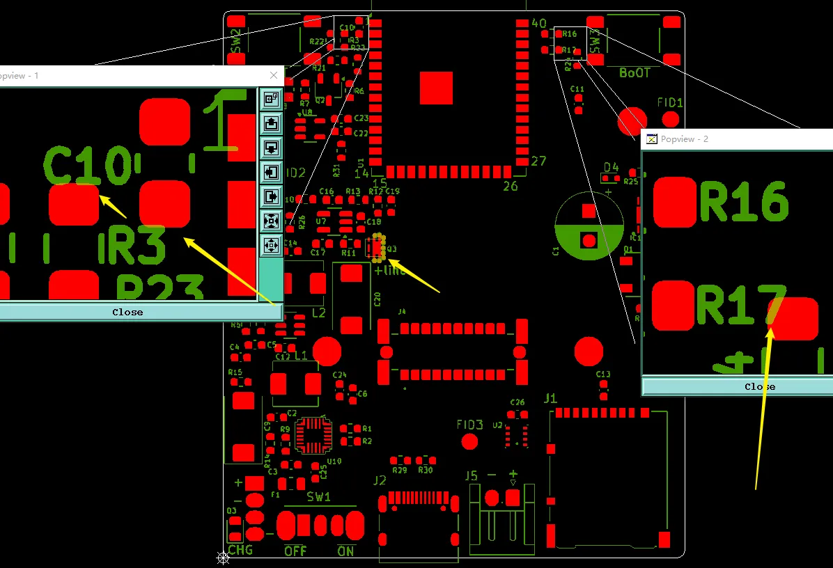
Designers select one finish (e.g. ENIG) on the instant quote but the uploaded files still contain notes or layer definitions for another finish (HASL or OSP). This is the single most common EQ across all three finishes.
Engineering Observation
CAM review consistently reveals discrepancies between order parameters and file content, especially when files are prepared before final finish selection.
Root Cause Analysis
Files are often based on old templates or default settings that are not updated when the quote finish is changed.
Design Impact
Incorrect plating leads to poor solderability, oxidation, or production rejection, causing delays and extra costs.
Recommended Solution
You chose [ENIG/HASL/OSP] but your file notes a different finish. Please advise which finish should be used.
Engineering Takeaway
Always ensure the surface finish selected on the quote exactly matches all notes and requirements in your Gerber files before submission.
Case 2: Gold Finger Compatibility Issues
Case Overview
Designs include gold fingers but the selected finish is HASL or OSP instead of ENIG.
Engineering Observation
Engineering review identifies gold finger features while the order specifies a non-immersion gold finish.
Root Cause Analysis
Gold fingers require ENIG or hard gold for reliable contact and wear resistance; HASL and OSP are incompatible.
Design Impact
Poor contact reliability, oxidation, and mechanical wear in edge connector applications.
Recommended Solution
There is design of gold finger, but you chose HASL/OSP. Should we change to ENIG and chamfer the edge?
Engineering Takeaway
Gold fingers must use ENIG. Always align surface finish with connector features during design.
Case 3: Via Tenting and Solder Mask Conflicts
Case Overview
Via tenting or covering specifications conflict between quote selection and actual solder mask layers, especially common when switching between ENIG, HASL, and OSP.
Engineering Observation
CAM review shows quote says tenting while files show open vias (or vice versa).
Root Cause Analysis
Mismatch between online quote parameters and Gerber solder mask layers.
Design Impact
Solder mask ink in holes or exposed vias causing assembly defects.
Recommended Solution
You chose Vias Tenting but file shows Not Covered. Please advise which to follow.
Engineering Takeaway
Always synchronize via treatment between quote and solder mask layers regardless of finish type.
Case 4: Silkscreen on Pads and BGA Compatibility
Case Overview
Silkscreen placed on SMD pads or BGA pads sized too small for the chosen finish.
Engineering Observation
DFM flags silkscreen overlap and undersized pads, particularly problematic with HASL and ENIG.
Root Cause Analysis
Designers do not adjust for finish-specific plating and assembly requirements.
Design Impact
Poor solderability, weak joints, and assembly defects.
Recommended Solution
Characters designed on pads or BGA pads too small. Please advise to delete/move or enlarge.
Engineering Takeaway
Keep silkscreen off pads and ensure adequate pad sizes for the chosen surface finish (especially ENIG and HASL).
Practical Best Practices to Minimize EQ When Choosing Surface Finish
1. Cross-check quote finish selection with all Gerber notes and layers before upload. 2. Use ENIG for boards with gold fingers or fine-pitch components. 3. Use HASL for cost-sensitive, larger-pitch designs with good thermal requirements. 4. Use OSP for very cost-sensitive, short shelf-life applications with single reflow. 5. Always request a free DFM review when changing surface finish.
Conclusion
Choosing the right surface finish for FR4 PCBs is critical for both performance and manufacturability. By understanding the common EQs for ENIG, HASL, and OSP and following the design rules above, you can significantly reduce engineering clarifications and achieve better production outcomes. For real production records across these finishes, visit our Production Records. Ready to start your project? Get a Quote today and let our engineering team provide a full DFM review.
FAQs
Q1: Which surface finish is best for gold fingers?
A1: ENIG is required. HASL and OSP are not suitable for reliable edge connector performance.
Q2: Can I change surface finish after uploading files?
A2: Yes, but it often requires EQ and may need file updates. Best to confirm before upload.
Q3: What is the main advantage of OSP over HASL?
A3: Lower cost and flatter surface, but shorter shelf life and limited to fewer reflow cycles.
Q4: Should vias be tented for all three finishes?
A4: It depends on your design intent. Clearly specify and keep consistent between quote and files.
References
IPC-6012E — Qualification and Performance Specification for Rigid Printed Boards.