Introduction
Although 1 Layer FR4 PCBs (single-sided boards) are among the simplest PCB types, they still generate a surprising number of Engineering Queries during CAM review and production. Single-sided designs are widely used in cost-sensitive applications such as LED lighting, consumer electronics, power supplies, and basic control boards where only one copper layer is required for routing.
In actual engineering file reviews, factory teams frequently encounter issues related to hole attributes, silkscreen placement, solder mask coverage, and mechanical features. These problems arise because designers often apply rules suitable for double-sided or multilayer boards without adjusting for single-layer manufacturing constraints. Resolving these EQs early prevents unnecessary delays, reduces scrap rates, and ensures reliable assembly even on the most basic boards.
This article details the most common real-world EQs observed in 1 Layer FR4 production, drawn directly from CAM experience and order data, and provides clear design-side prevention strategies.
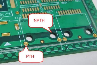
Case 1: Single-Sided Boards Can Only Use NPTH Holes
Case Overview
In many 1 Layer FR4 designs, files include notes or drill definitions requesting plated through holes (PTH), even though only one copper layer exists. This is especially common when designers copy templates from double-sided projects or when files contain legacy comments about copper plating.
Engineering Observation
During DFM review, the CAM team identifies PTH attributes or notes in single-sided Gerber files that cannot be physically realized because there is no copper on the opposite side.
Root Cause Analysis
Designers often overlook that single-sided boards lack the second copper layer required for plating through holes, leading to conflicting instructions between the drill file and actual layer stack.
Design Impact
Attempting to plate non-existent holes can cause production errors, incorrect hole finishing, or rejection of the entire order, increasing both cost and lead time.
Recommended Solution
Since we can only make Non-plated through holes on single-side boards, should we ignore the note in your file requesting plated holes? 1. ignore the note and accept NPTH or 2. please advise.
Engineering Takeaway
On all 1 Layer FR4 PCBs, holes must be designed as Non-Plated (NPTH). Remove any PTH requirements or plating notes to avoid unnecessary EQs and production issues.
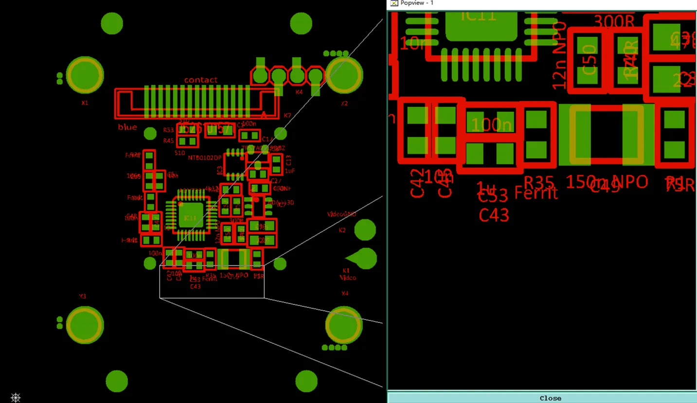
Case 2: Silkscreen Characters on SMD Pads
Case Overview
Component legends and markings are frequently placed directly on solder pads in 1 Layer FR4 designs to save space or improve readability during manual assembly.
Engineering Observation
DFM checks show silkscreen overlapping copper pads, particularly on larger components and connectors common in single-sided boards.
Root Cause Analysis
Designers prioritize visual guidance without considering that silkscreen ink on pads interferes with solder paste deposition and final joint formation.
Design Impact
This leads to poor solderability, weak joints, tombstoning, or visible defects that affect both appearance and reliability in the final product.
Recommended Solution
As shown in the picture, the characters (component name) are designed on the pads. Please advise whether we can delete them or move the characters to proper position: 1. delete and accept broken characters or 2. move to proper position.
Engineering Takeaway
Never place silkscreen on SMD pads in 1 Layer FR4 designs. Keep all legend markings clear of copper features to guarantee reliable soldering.
Case 3: Solder Mask Coverage on Single-Sided Boards
Case Overview
Designs sometimes omit solder mask entirely or apply full coverage that blocks component soldering areas on 1 Layer FR4 boards.
Engineering Observation
CAM review identifies missing solder mask layers or full-board coverage that would prevent proper component attachment.
Root Cause Analysis
Single-sided files are often simplified from double-sided templates without properly defining solder mask openings for pads and through holes.
Design Impact
Without correct solder mask, components cannot be soldered reliably, leading to assembly failures or the need for manual rework.
Recommended Solution
If we cover solder mask ink on the whole board, all the plated through holes indicated will not be able to weld components. Please advise: 1. do as per file and cover solder mask or 2. revise the file to add proper openings.
Engineering Takeaway
Always provide complete solder mask layers with proper openings for all pads on 1 Layer FR4 PCBs. Full coverage without openings makes assembly impossible.
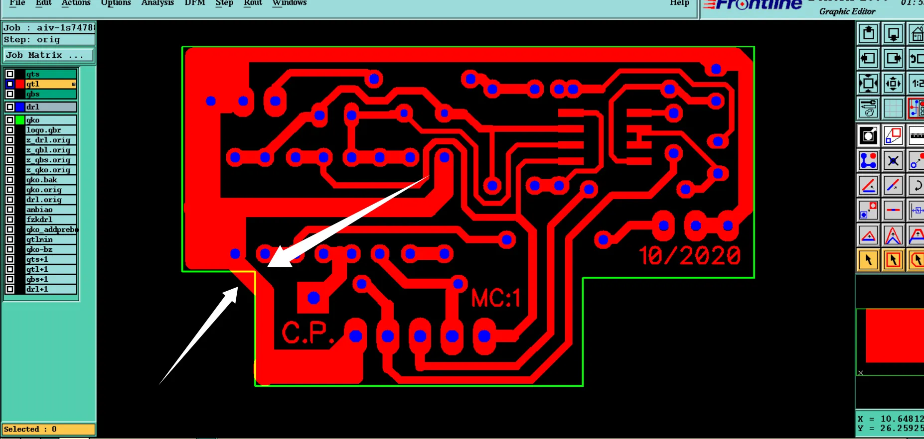
Case 4: Pads and Traces Too Close to Board Edge
Case Overview
Component pads and traces are placed very close to the routed board edge in 1 Layer FR4 designs to maximize usable area.
Engineering Observation
DFM analysis shows pads or traces within 0.2mm of the outline, which risks damage during mechanical routing.
Root Cause Analysis
Designers do not account for routing tolerance and material behavior on single-sided boards where there is no second side for support.
Design Impact
Routing can cause exposed copper, burrs, lifted pads, or damaged traces, affecting both cosmetic quality and electrical performance.
Recommended Solution
The spacing between the pad/trace and the edge of the board is too close, which will lead to copper leakage if we do as per file. Please advise whether you can accept copper leakage or need design revision.
Engineering Takeaway
Maintain sufficient clearance (minimum 0.2mm for routed edges) between pads/traces and the board outline on 1 Layer FR4 designs.
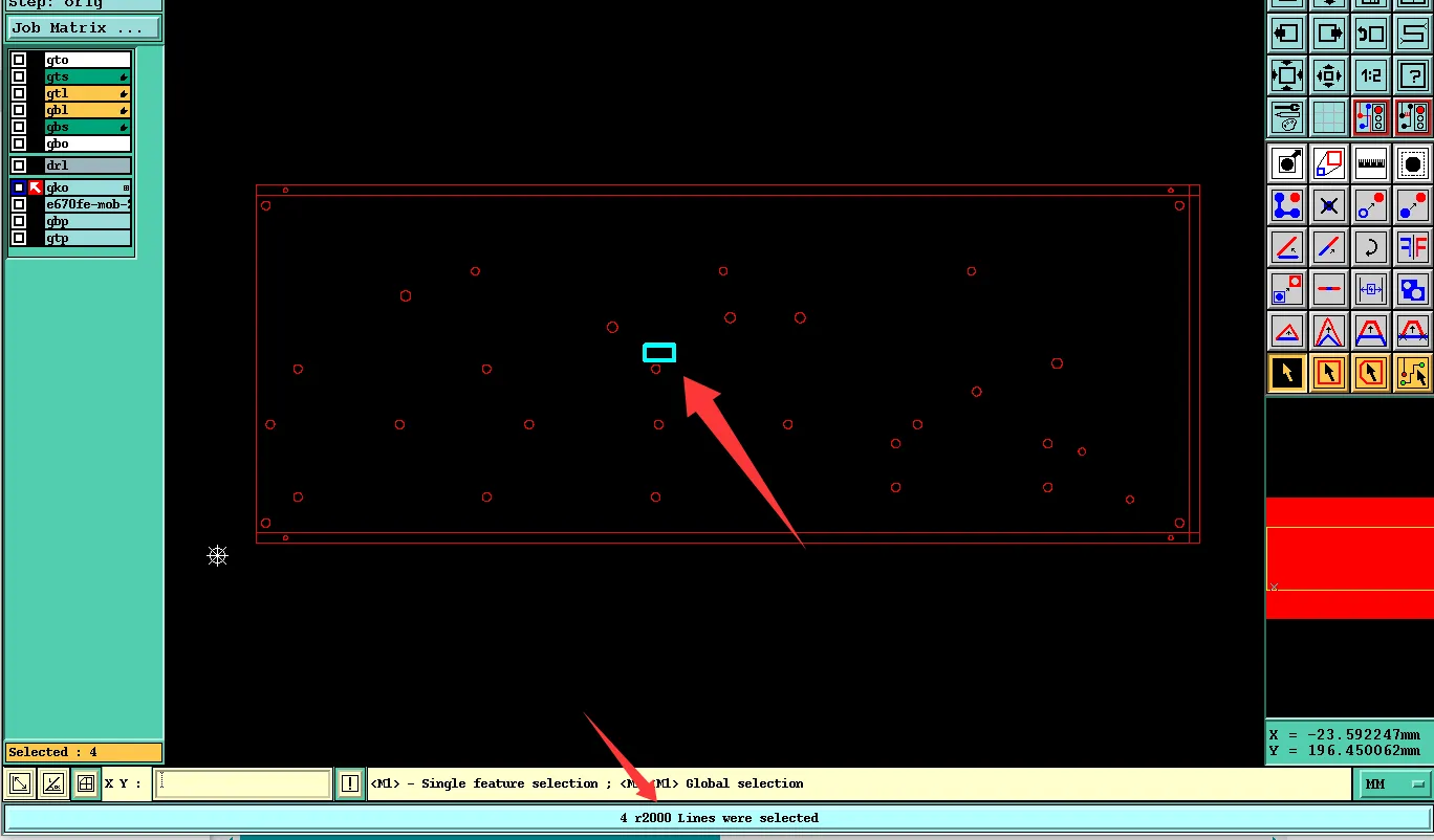
Case 5: Outline Dimension Ambiguity with Wide Lines
Case Overview
GKO or mechanical layers use thick outline lines, making the final board dimension unclear.
Engineering Observation
CAM cannot determine whether to follow the center, inner, or outer edge of wide outline lines.
Root Cause Analysis
Design software often outputs thick mechanical layers without explicit dimension intent for simple single-sided boards.
Design Impact
Incorrect final dimensions cause fitment problems in enclosures or complete board rejection.
Recommended Solution
The width of outline in GKO layer is too wide. Please advise which dimension we should follow: inner, center, or outer.
Engineering Takeaway
When using wide outline lines in 1 Layer FR4 designs, clearly specify the intended final board dimensions in notes or documentation.
Practical Best Practices to Minimize EQ
1. Always design holes as NPTH on 1 Layer FR4 and remove any PTH-related notes. 2. Keep silkscreen completely off SMD pads and maintain proper clearances. 3. Provide complete solder mask layers with accurate openings for all pads. 4. Maintain adequate edge clearance (≥0.2mm) for pads and traces. 5. Clearly define final board dimensions when using thick outline lines. 6. Refer to our 1 Layer FR4 PCB Manufacturing Insights page before finalizing your design and request a free DFM review.
Conclusion
Even simple 1 Layer FR4 PCBs require careful attention to hole attributes, silkscreen, solder mask, and mechanical features to avoid common EQs. By following the design rules outlined above, engineers can achieve smoother production, higher yield, and faster delivery. For real production examples of stable single-sided board delivery, visit our Production Records. Ready to proceed with your 1 Layer FR4 project? Get a Quote today or upload your files for a complimentary engineering review.
FAQs
Q1: Can 1 Layer FR4 PCBs have plated through holes?
A1: No. Single-sided boards can only use Non-Plated (NPTH) holes. Always design accordingly and remove PTH notes.
Q2: Should silkscreen be placed on component pads?
A2: No. Keep all legend markings clear of pads to ensure reliable soldering.
Q3: How close can pads be to the board edge on 1 Layer FR4?
A3: Maintain at least 0.2mm clearance from routed edges to avoid copper exposure and burrs.
Q4: Do I need to provide a full solder mask layer for single-sided boards?
A4: Yes. Proper solder mask openings are essential for component soldering and protection.
Q5: What files should I prepare for 1 Layer FR4 orders?
A5: Complete Gerber set with NPTH holes, proper solder mask, clear outline dimensions, and no silkscreen on pads. Request DFM review from AIVON.
References
IPC-6012E — Qualification and Performance Specification for Rigid Printed Boards.