Most Common Engineering Queries in 2 Layer FR4 PCB Production
2 Layer FR4 PCBs (double-sided boards) are one of the most widely used PCB types, striking an excellent balance between cost, complexity, and functionality. They are commonly found in consumer electronics, industrial controls, power supplies, and LED drivers where routing on both sides and plated through holes are required.
Despite their relative simplicity compared to multilayer boards, 2 Layer FR4 designs still generate a high volume of Engineering Queries during CAM review. In actual production, factory teams frequently encounter mismatches in via treatment, silkscreen placement, solder mask openings, hole attributes, and edge clearance. These issues often stem from designers applying general rules without fully considering double-sided manufacturing constraints and process tolerances.
This article presents the most common real-world EQs observed in 2 Layer FR4 production, drawn directly from CAM experience and order data. It provides clear, actionable design-side prevention strategies to help engineers reduce back-and-forth communication and achieve higher first-pass success rates.
| Case | Issue | Common Impact |
|---|---|---|
| 1 | Via Tenting Mismatch | Solder wicking or blocked holes |
| 2 | Silkscreen on SMD Pads | Poor solderability and tombstoning |
| 3 | Solder Mask Bridge Spacing | Shorts or exposed traces |
| 4 | Edge Clearance Violations | Copper burrs or lifted pads |
| 5 | PTH vs NPTH Ambiguity | Plating errors and assembly issues |
Case 1: Via Tenting vs Open Specification Mismatches in 2 Layer FR4 Designs
Case Overview
In 2 Layer FR4 designs, vias are often specified with tenting or covering requirements on the quote page, but the actual Gerber solder mask layers show conflicting definitions (open or covered). This mismatch is extremely common when designers transition from single-sided or template-based files.
Engineering Observation
During DFM review, the CAM team identifies clear differences between the selected via treatment on the instant quote and the solder mask layers in the production files.
Root Cause Analysis
Many designers select Via Tenting on the quote without updating the solder mask layers in Gerber files, or they use default templates that do not match the final process choice.
Design Impact
Incorrect via covering can cause solder mask ink to enter holes (blocking them) or leave vias exposed, leading to solder wicking, shorts during assembly, or reliability issues in the field.
Recommended Solution
You chose Vias Tenting on the instant quote page, but in your file it is Vias Not Covered. Please advise: 1. do as chosen (Tenting) or 2. do as per file (Not Covered). Proper alignment between quote and files is essential for consistent results.
Engineering Takeaway
Always ensure via tenting or covering specifications are consistent between your quote selection and the actual solder mask layers in Gerber files for 2 Layer FR4 designs.
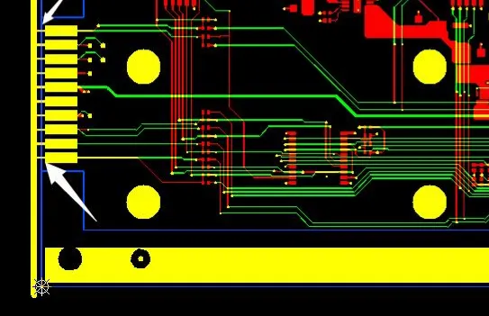
Case 2: Silkscreen Overlapping SMD Pads on Double-Sided FR4 Boards
Case Overview
Component reference designators and markings are frequently placed directly on SMD pads in 2 Layer FR4 layouts to improve readability during assembly and debugging.
Engineering Observation
DFM checks routinely flag silkscreen overlapping copper pads, especially on fine-pitch components and connectors.
Root Cause Analysis
Designers prioritize visual clarity without accounting for the impact of silkscreen ink on solder paste application and final joint formation with HASL or ENIG finishes.
Design Impact
Silkscreen on pads leads to poor solderability, tombstoning, weak joints, or visible defects that can cause both assembly failures and customer quality concerns.
Recommended Solution
As shown in the picture, the characters (component name) are designed on the pads. Please advise whether we can delete them or move the characters to proper position: 1. delete and accept broken characters or 2. move to proper position.
Engineering Takeaway
Never place silkscreen on SMD pads in 2 Layer FR4 designs. Maintain adequate clearance from all copper features to ensure reliable soldering and high assembly yield.
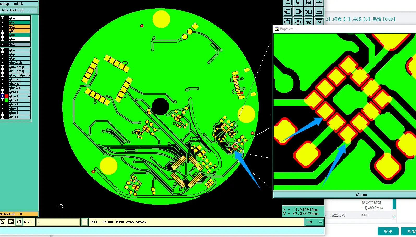
Case 3: Insufficient Solder Mask Bridge Spacing on Fine-Pitch Pads
Case Overview
IC or fine-pitch pads in 2 Layer FR4 designs often have insufficient spacing for solder mask bridges, or openings are misaligned with pads.
Engineering Observation
CAM review identifies areas where solder mask bridges cannot be reliably formed or openings do not match pad locations.
Root Cause Analysis
Designers sometimes use minimum pad spacing suitable for theoretical layouts without considering actual solder mask registration and process tolerances.
Design Impact
Insufficient solder mask bridges can cause shorts during assembly, while misaligned openings lead to exposed traces or poor protection.
Recommended Solution
The spacing between IC's pads is too small to do solder mask bridge. Please advise whether we can remove the solder mask bridge and make solder mask full opening or revise the file to increase spacing.
Engineering Takeaway
Ensure adequate spacing between pads (typically ≥0.23mm for bridges) in 2 Layer FR4 designs to allow reliable solder mask bridges and prevent shorts.
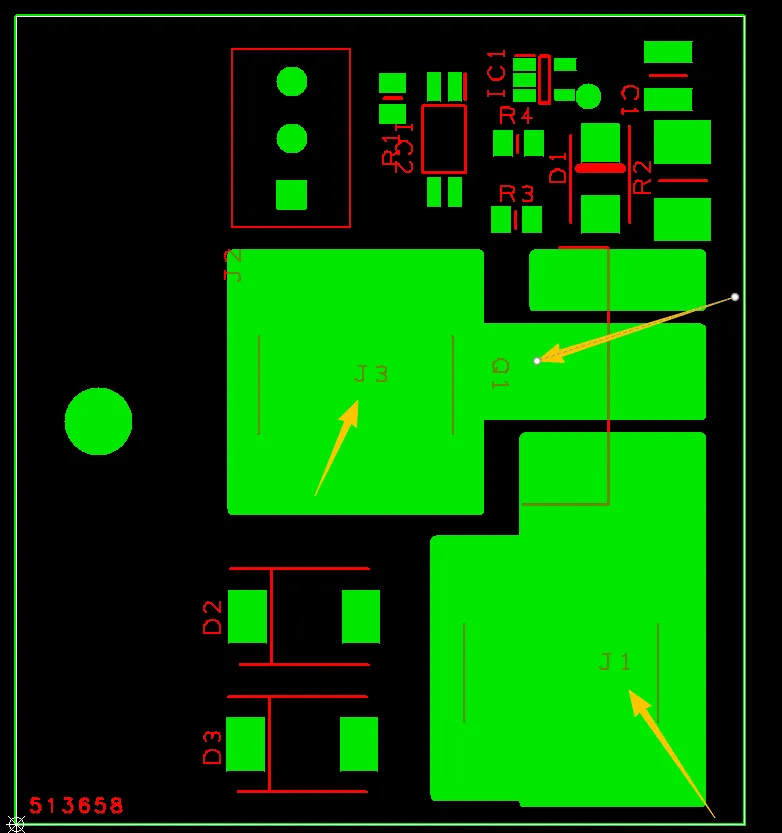
Case 4: Pads and Traces Too Close to Board Outline in 2 Layer FR4 PCBs
Case Overview
Component pads and traces are placed too close to the routed or V-cut board edge to maximize board utilization.
Engineering Observation
DFM analysis shows pads/traces within critical distance of the outline, risking damage during mechanical processing.
Root Cause Analysis
Designers do not always account for routing and V-cut tolerances on double-sided boards where mechanical stress is higher.
Design Impact
Routing or V-cutting can cause exposed copper, burrs, lifted pads, or damaged traces, affecting both quality and electrical performance.
Recommended Solution
The spacing between the pad/trace and the edge of the board is too close. This will lead to copper leakage. Please advise whether you can accept copper leakage or need design revision (e.g., cut off part of the pad).
Engineering Takeaway
Maintain minimum clearance (≥0.2mm for routed edges, ≥0.4mm for V-cut) between pads/traces and the board outline on 2 Layer FR4 designs.
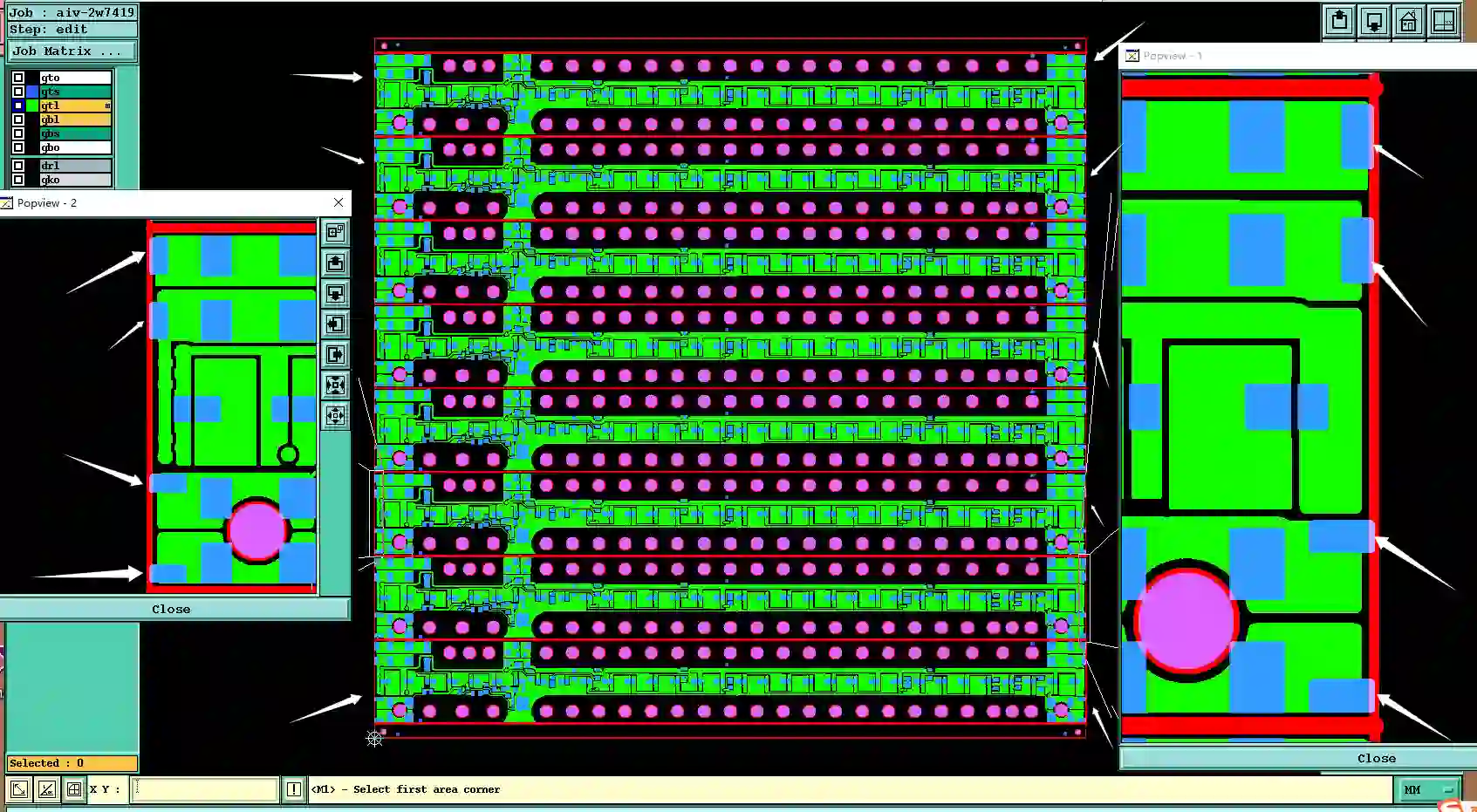
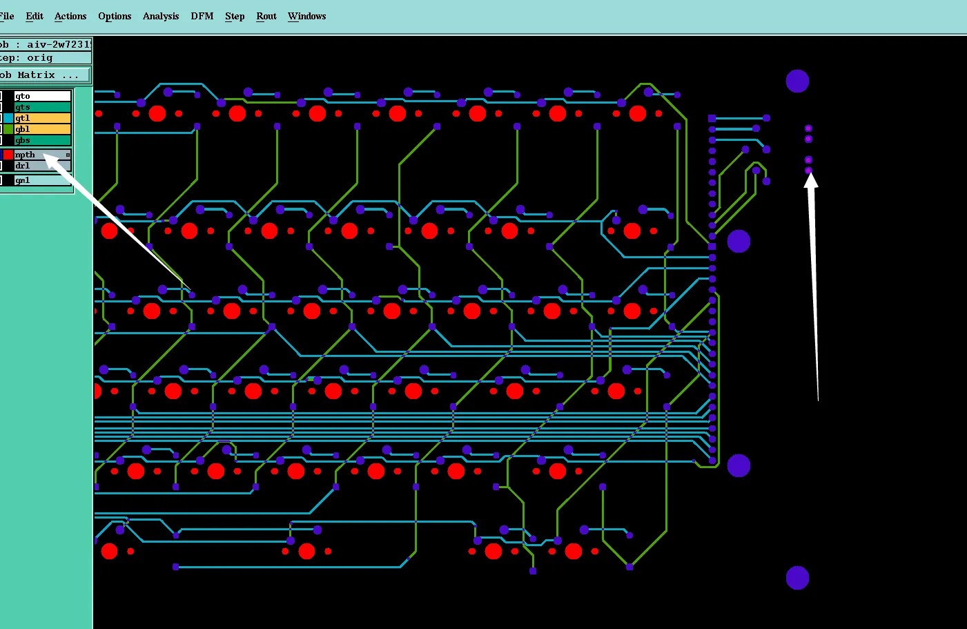
Case 5: Ambiguous PTH vs NPTH Hole Definitions in Gerber Files
Case Overview
2 Layer FR4 designs frequently contain ambiguous hole attributes, with drill drawings and Gerber files showing conflicting PTH/NPTH definitions.
Engineering Observation
CAM review identifies holes defined as NPTH in drill tables but with pads on both sides, or vice versa.
Root Cause Analysis
Design tools and copy-paste practices often result in unclear plating specifications, especially when mixing mounting holes and vias.
Design Impact
Incorrect plating decisions lead to shorts, opens, assembly problems, or unreliable electrical connections.
Recommended Solution
Please advise whether the indicated holes should be Plated through holes or Non-plated through holes. Clear definition prevents downstream manufacturing errors.
Engineering Takeaway
Clearly specify plating requirements (PTH or NPTH) for every hole type in 2 Layer FR4 Gerber files and drill drawings.
DFM Best Practices to Reduce Common EQs on 2 Layer FR4 PCBs
- Always align via tenting/covering choices between quote and solder mask layers.
- Keep silkscreen completely away from all SMD pads.
- Maintain proper clearances from board edges and ensure solder mask bridges where needed.
- Clearly define PTH vs NPTH attributes for every hole.
- Provide complete, consistent Gerber files and request a free DFM review from AIVON early.
- Refer to our 2 Layer FR4 PCB Manufacturing Insights page for detailed process guidelines before finalizing your design.
Conclusion
2 Layer FR4 PCBs are foundational but still require careful attention to via treatment, silkscreen, solder mask, and mechanical details to avoid common EQs. By implementing the design rules and best practices above, engineers can achieve smoother production runs, higher yields, and faster delivery. For real production examples of stable 2 Layer FR4 delivery, visit our Production Records. Ready to proceed? Get a Quote today or upload your files for a complimentary engineering review.
FAQs
Q1: Should vias be tented or left open on 2 Layer FR4 boards?
A1: Clearly specify your preference on both the quote and in solder mask layers. Consistent documentation prevents one of the most frequent EQs.
Q2: Can I place silkscreen on component pads?
A2: No. Keep all legend markings clear of pads to ensure reliable soldering and assembly.
Q3: How close can pads be to the board edge?
A3: Maintain at least 0.2mm for routed edges and 0.4mm for V-cut to avoid copper exposure and burrs.
Q4: Do I need to clearly label PTH vs NPTH holes?
A4: Yes. Ambiguous hole attributes are a very common EQ on 2 Layer boards. Use clear drill drawing notations.
Q5: What files should I prepare before submitting a 2 Layer FR4 order?
A5: Complete Gerber set with consistent via treatment, proper solder mask, clear hole attributes, and no silkscreen on pads. Request DFM review from AIVON.
References
IPC-6012E — Qualification and Performance Specification for Rigid Printed Boards.