Introduction
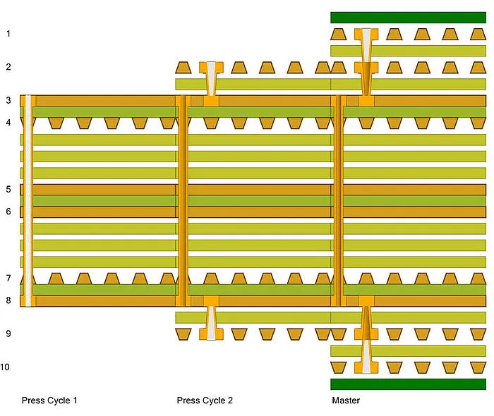
Sequential lamination represents a critical manufacturing technique for producing high-performance printed circuit boards, particularly those with high layer counts and complex interconnect structures. This process involves multiple lamination cycles to build up layers incrementally, enabling the integration of blind and buried vias while maintaining precise alignment. Proper material selection plays a pivotal role in optimizing sequential lamination PCB materials, as it directly impacts thermal stability, signal integrity, and overall board reliability. Engineers must prioritize materials that withstand repeated thermal excursions without compromising structural integrity or electrical performance. In high-performance applications, such as telecommunications and computing systems, suboptimal choices can lead to issues like delamination or warpage. This guide explores key considerations for selecting sequential lamination PCB materials, focusing on thermal and dielectric properties to achieve robust designs.
High-Tg PCB laminates emerge as a cornerstone for these processes, offering enhanced resistance to elevated temperatures encountered during multiple press cycles. Similarly, low Dk PCB materials sequential lamination ensures minimal signal loss in high-speed circuits. Addressing CTE mismatch PCB lamination remains essential to prevent mechanical stresses that arise from differential expansion between copper and dielectrics. By aligning material properties with process demands, manufacturers can produce boards that meet stringent performance criteria. Factory-driven insights reveal that consistent material behavior across cycles is non-negotiable for yield optimization.
What Is Sequential Lamination and Why It Matters
Sequential lamination refers to a multilayer PCB fabrication method where cores and prepregs are laminated in successive stages rather than a single cycle. This approach accommodates the drilling, plating, and imaging of inner layers before outer layer bonding, facilitating high-density interconnects. It proves indispensable for boards exceeding 20 layers or those requiring stacked microvias. The technique allows for tighter control over layer registration, reducing misalignment risks inherent in all-at-once lamination. For electric engineers designing high-performance systems, understanding sequential lamination PCB materials becomes crucial to leverage its advantages fully.
The relevance stems from the escalating demands of modern electronics for denser routing and faster signals. Traditional single-lamination struggles with thick stacks, leading to voids or incomplete fills. Sequential methods mitigate these by distributing thermal and pressure loads across cycles. However, they amplify material challenges, as each cycle exposes laminates to heat and pressure repeatedly. Poor selection exacerbates defects like via barrel cracking or board bowing. Industry practices emphasize materials engineered for multi-cycle stability to ensure long-term reliability in demanding environments.
Key Material Properties for Sequential Lamination PCB Materials
Selecting sequential lamination PCB materials hinges on balancing thermal, mechanical, and electrical characteristics. Thermal properties govern stability during press cycles, where temperatures often exceed standard curing points. Dielectric attributes dictate signal propagation, vital for high-frequency performance. Mechanical resilience counters stresses from repeated processing. Engineers evaluate these holistically to avoid compromises in yield or functionality.
Thermal Properties: Tg and CTE Considerations
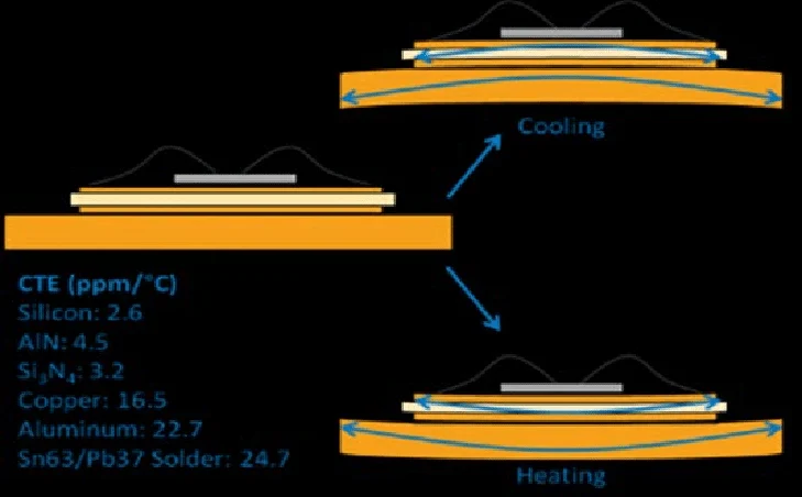
Glass transition temperature, or Tg, marks the point where the laminate shifts from glassy to rubbery state, influencing flow and adhesion. High-Tg PCB laminates maintain rigidity at elevated temperatures, reducing resin flow inconsistencies across cycles. Coefficient of thermal expansion, CTE, measures dimensional change with heat, critical for multilayer harmony. Z-axis CTE, in particular, demands close matching to copper foil to avert cracks. Low Z-axis expansion materials prove ideal for sequential builds.
Dielectric Properties: Dk and Df
Dielectric constant, Dk, affects impedance and crosstalk in high-speed traces. Low Dk PCB materials sequential lamination preserve signal speed by minimizing capacitance. Dissipation factor, Df, quantifies energy loss, where lower values enhance efficiency. These properties remain stable only in materials formulated for thermal cycling. Selection prioritizes consistency post-lamination to sustain performance.
Mitigating CTE Mismatch in PCB Lamination
CTE mismatch PCB lamination arises when dielectric and conductor expansions diverge, inducing shear stresses at interfaces. During cooling from lamination temperatures, higher CTE in resins relative to copper generates tensile forces on vias and pads. Repeated cycles compound this, risking delamination or microcracks. Factory monitoring focuses on symmetric stackups to symmetrize stresses. Material choices with tailored CTE profiles across X, Y, and Z axes distribute loads evenly.
IPC-6012 establishes performance benchmarks, including warpage tolerances that underscore CTE control. Prepreg-core combinations must exhibit compatible expansion to pass qualification. Process aids like carrier plates during pressing further stabilize dimensions. Engineers simulate thermal profiles to predict mismatch impacts pre-production.
Selecting High-Tg PCB Laminates for Sequential Processes
High-Tg PCB laminates excel in sequential lamination by resisting softening during multiple heats. These materials sustain structural integrity, ensuring uniform prepreg flow without excessive squeeze-out. They also exhibit lower moisture absorption, minimizing voids from vaporization. Compatibility with lead-free profiles extends their utility in modern assembly. Selection involves verifying multi-cycle performance data from suppliers.
Pairing high-Tg cores with matching prepregs prevents interlayer slippage. Resin systems in these laminates offer higher modulus above Tg, bolstering mechanical strength. For high-performance PCBs, this translates to superior via reliability under thermal shock.
Integrating Low Dk PCB Materials in Sequential Lamination
Low Dk PCB materials sequential lamination support high-frequency designs by reducing propagation delays. These resins, often with reinforced fillers, maintain low permittivity through thermal excursions. Challenges include higher costs and processing sensitivities, yet benefits outweigh for RF and data applications. Sequential builds allow embedding these in inner layers for optimal shielding.
Balancing low Dk with thermal stability requires hybrid stacks, blending standard and advanced materials judiciously. Df stability prevents skew in differential pairs. Factory validation confirms no degradation post-cycles.
Best Practices for Material Selection and Process Optimization
Effective sequential lamination demands rigorous material vetting aligned with factory capabilities. Begin with defining performance tiers based on end-use, prioritizing high-Tg PCB laminates for thermal demands and low Dk variants for speed. Conduct compatibility trials for CTE matching across the stack.
- Evaluate resin flow and gel time for void-free bonds.
- Use symmetric constructions to counter bow and twist.
- Implement carrier-based pressing for thin cores.
- Monitor press parameters like ramp rates to avoid hotspots.
IPC-4101 outlines laminate specifications, guiding selections for consistent behavior. Post-lamination inspections verify flatness and continuity.
Property: High Tg; Sequential Lamination Priority: Essential; Rationale: Multi-cycle thermal resistance.
Property: Low Z-CTE; Sequential Lamination Priority: Critical; Rationale: Minimize via stress.
Property: Low Dk/Df; Sequential Lamination Priority: Application-specific; Rationale: Signal integrity.
Property: Low Moisture Absorption; Sequential Lamination Priority: Recommended; Rationale: Prevent voids.
Common Challenges and Troubleshooting Insights
Warpage tops challenges in CTE mismatch PCB lamination, often from asymmetric builds or mismatched materials. Troubleshooting starts with stackup redesign for balance. Delamination signals excessive flow or contamination, addressed by plasma cleaning prepregs. Via failures trace to plating inconsistencies post-drilling.
Sequential processes amplify drill smear risks, mitigated by optimized feeds. Yield data guides iterative refinements. Standard-aligned practices ensure repeatability.
Conclusion
Optimizing sequential lamination PCB materials hinges on precise selection of high-Tg PCB laminates, low Dk options, and CTE-matched combinations. These choices fortify boards against thermal and mechanical rigors of multi-cycle builds. Factory insights underscore proactive stackup planning and process controls for peak performance. Electric engineers benefit from integrating these principles early in design. Ultimately, informed material decisions yield reliable high-performance PCBs ready for demanding applications.
FAQs
Q1: What role do high-Tg PCB laminates play in sequential lamination PCB materials?
A1: High-Tg PCB laminates provide thermal stability during multiple lamination cycles, preventing resin softening and ensuring uniform bonding. They reduce risks of delamination and maintain dimensional control under heat. Factory processes favor them for high-layer counts, aligning with performance needs in complex builds.
Q2: How does CTE mismatch affect PCB lamination outcomes?
A2: CTE mismatch PCB lamination induces stresses leading to warpage, via cracks, or interlayer separation during thermal cycling. Matching Z-axis CTE of dielectrics to copper minimizes these issues. Symmetric stackups and low-expansion materials enhance reliability in sequential processes.
Q3: Why choose low Dk PCB materials for sequential lamination?
A3: Low Dk PCB materials sequential lamination preserve signal speed and reduce losses in high-frequency designs. They maintain dielectric stability across cycles, crucial for RF and data integrity. Selection balances with thermal properties for overall stack performance.
Q4: What standards guide sequential lamination material selection?
A4: IPC-4101 and IPC-6012 provide benchmarks for laminate properties and board performance in sequential lamination. They specify thermal, mechanical, and warpage criteria. Adhering ensures factory-consistent results without defects.
References
IPC-4101E — Specification for Base Materials for Rigid and Multilayer Printed Boards. IPC, 2010
IPC-6012E — Qualification and Performance Specification for Rigid Printed Boards. IPC, 2017
IPC-2221B — Generic Standard on Printed Board Design. IPC, 2012