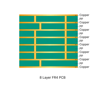
8 Layer FR4 PCB Production Record #FR4-20260115-007
| Parameter | Value | Parameter | Value |
|---|---|---|---|
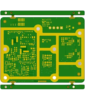
| PCB Type | FR4 PCB | Quantity | 10 pcs |
| Layers | 8 Layers | Board Type | Panel PCB |
| Dimensions | 77.5 x 60 mm | Copper Weight | 1oz |
| Thickness | 1.6 mm | Min Track / Spacing | 5/5mil |
| Surface Finish | ENIG (Immersion Gold) | Min Hole Size | 0.1mm |
| Solder Mask | Green | Silkscreen | White |
| Stack-up | Custom | Impedance Control | No |
This 8-layer FR-4 PCB was built on TG170 material with a finished thickness of 1.6 mm and overall dimensions of 77.5 × 60 mm. The stack featured 0.5 oz outer copper and 1 oz inner layers, 0.1 mm minimum hole size, 5 mil line/space, and blind/buried vias. Ten pieces were produced as single boards with ENIG surface finish and delivered after 100% flying probe testing within a 9-day lead time. The presence of buried vias (layers 2-7) and tight geometry required careful stackup planning and lamination control to maintain registration and interlayer reliability.
DFM and EQ communications addressed several file discrepancies. Customer-provided data showed conflicting board thickness values and an unopenable ODB file. Stackup was optimized with adjusted PP and core thicknesses using two separate cores to accommodate the buried via structure, while process edges were corrected from left-right to up-down orientation per production requirements. Markings including serial numbers and customer symbols were added on the top solder mask layer with copper-exposed openings after confirmation of Gerber-format details and white ink contrast. These stackup optimization and process edge adjustments ensured manufacturability without compromising via reliability or dimensional accuracy.
All ten boards passed final electrical testing, micro-section analysis, and visual inspection. Delivered with test reports, certificate of conformity, and confirmed stackup documentation. The order was completed with stable thickness control and clean via formation on this compact, high-layer-count configuration.
These boards integrate multiple microvia layers to support complex routing and high signal density in advanced electronics.

In-depth guide to the most frequent Engineering Queries (EQ) and DFM issues in Multilayer FR4 PCB (4/6/8+ layers) production. Real factory insights on stack-up confirmation, impedance control, copper balance, inner layer design, via treatment, registration, and practical prevention strategies.
| Order ID | PCB Type | Layers | Dimensions | Solder Mask | Surface Finish | Quantity | Action |
|---|---|---|---|---|---|---|---|
| FR4-20260520-046 | FR4 PCB | 2 | 94.21 x 275 | Green | ENIG (Immersion Gold) | 75 | View detail |
| FR4-20260519-001 | FR4 PCB | 10 | 67.6 x 42 | Green | Gold Plating | 20 | View detail |
| FR4-20260516-065 | FR4 PCB | 4 | 119 x 98 | Green | ENIG (Immersion Gold) | 20 | View detail |


