In February 2026, we processed a long and narrow 2-layer PCB order measuring 570 × 20 mm with an unusually thick 4 mm finished board. The design used FR-4 TG150 material, asymmetric copper weight (1oz/3oz), and HASL surface finish. Although only 2 layers, the extreme aspect ratio, thickness, and single-piece shipment requirement created several practical manufacturing challenges during CAM review.
Ultra-thick, narrow boards are particularly difficult to handle in production. Our CAM team identified multiple DFM issues related to panelization, via processing, and mechanical referencing that required customer clarification to avoid production delays and quality risks.
Order Overview
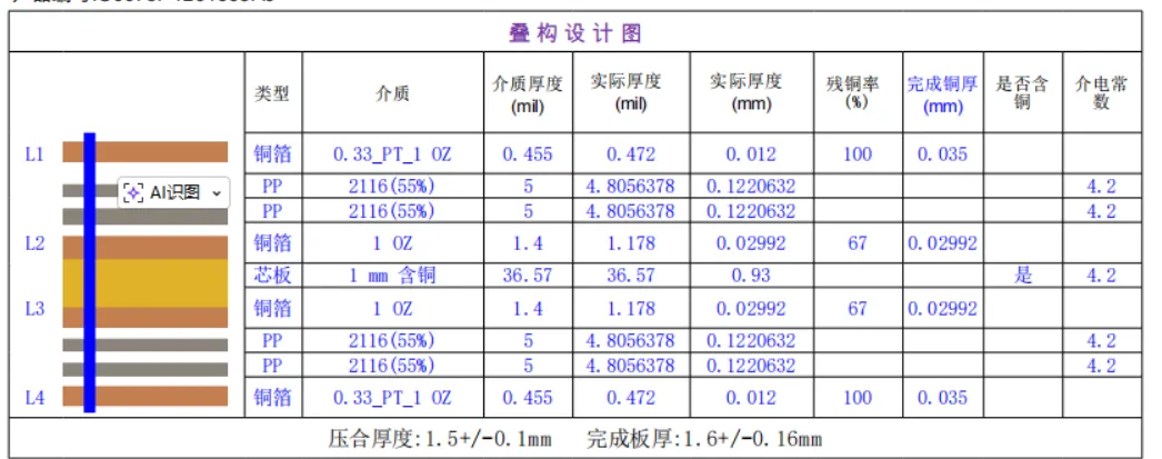
This was a 2-layer FR-4 TG150 PCB ( #FR4-20260314-020 ) with 1 oz outer copper and 3 oz inner copper, 4 mm finished thickness, and 0.5 mm minimum hole size. The board used HASL (lead-free) surface finish and required 100% flying probe testing. Specified as single-piece shipment with no panelization in the original data. Order quantity was 10 pcs (10 sets). The long, narrow profile combined with thick material made mechanical stability and processing accuracy critical concerns.
Main Engineering Questions Found During CAM Review
1. Panelization Strategy for Narrow Long Board
The customer specified single-piece delivery. However, with only 20 mm width, our engineer determined that individual processing would be highly inefficient and risk board warpage or handling damage. We suggested a 10-piece panel using stamp holes (0.8 mm holes with 0.25 mm spacing) for easy manual separation.
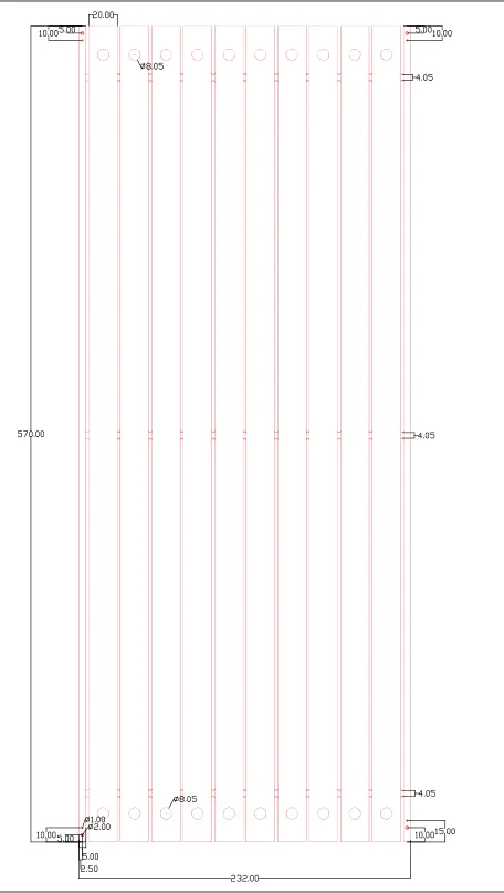
Figure 1: the width of a single pcs is only 20mm
We also proposed adding 2.0 mm locating holes and 1.0 mm fiducials on the process edges to improve registration and routing accuracy.
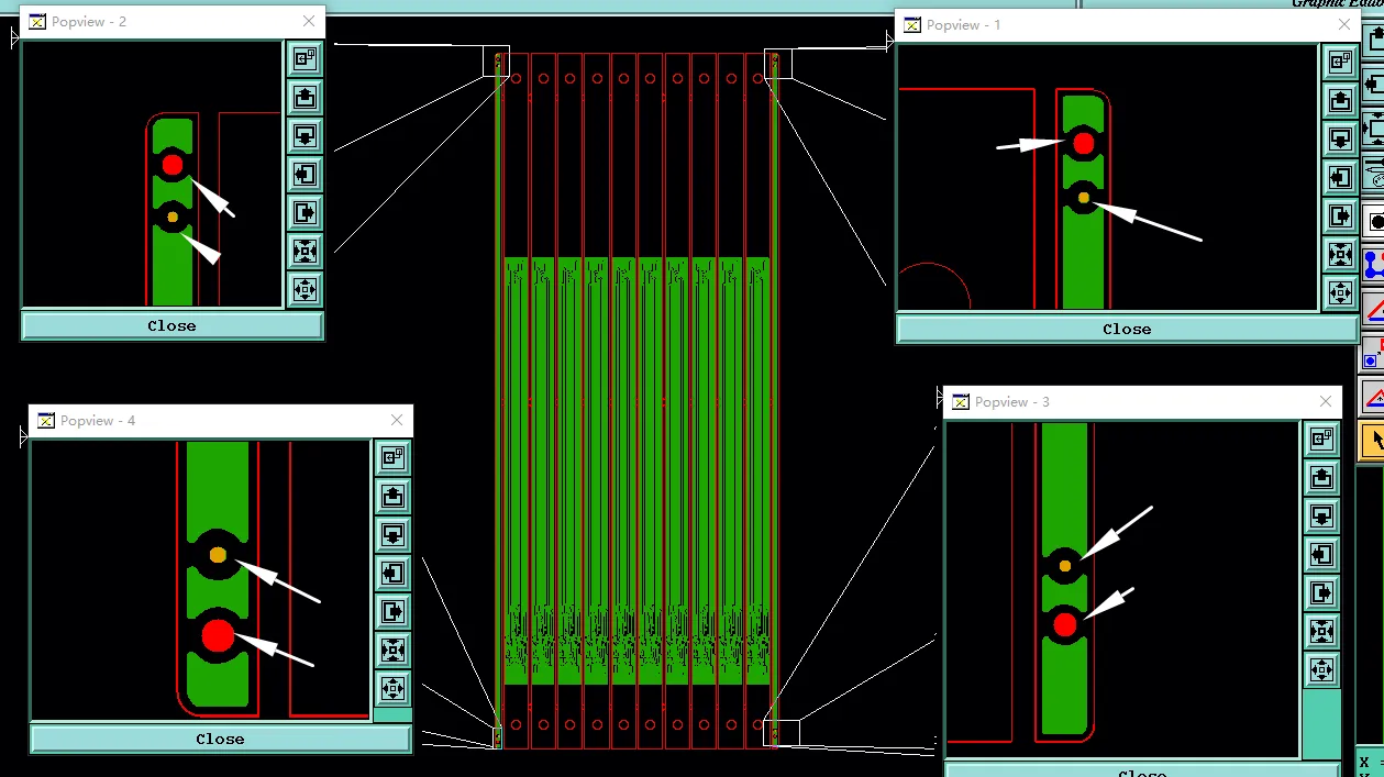
Figure 2: adding 2.0 mm locating holes and 1.0 mm fiducials on the process edges
If ignored and produced as single pieces without proper tooling, the narrow boards could suffer severe misalignment during drilling and routing, leading to dimensional inaccuracy and high scrap rates. Thick boards are especially prone to movement without adequate panel support.
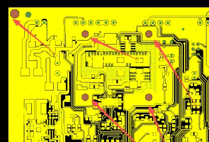
2. 0.4 mm Via Tenting on 4 mm Thick Board
The fabrication notes required tented (covered) vias for 0.4 mm holes. We noticed the high aspect ratio (hole depth to diameter) combined with thick material would make reliable tenting difficult. Ink could easily enter the holes, causing blockage and solder bead entrapment during assembly.
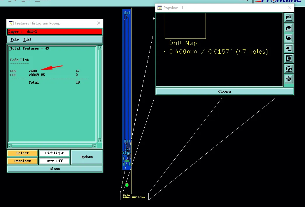
Figure 3: tented (covered) vias for 0.4 mm holes
Our CAM engineer recommended pre-drilling compensation to 0.6 mm to improve plating and tenting reliability while maintaining final hole size after plating. We asked for customer confirmation on this adjustment.
Without this optimization, vias could become partially or fully plugged with solder mask, trapping flux residue or solder balls, leading to reliability failures or assembly defects. In extreme cases, poor plating in high aspect ratio holes could cause open circuits.
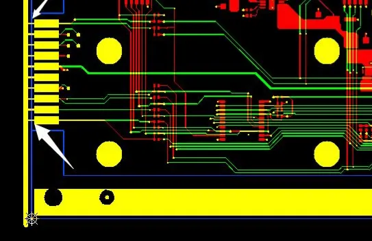
3. NPTH Hole Size and Tolerance Confirmation
Several non-plated holes were not explicitly sized in the data. Our team measured 8.05 mm from the outline and sought confirmation. We also clarified thickness tolerance (4 mm ±10% per IPC standards) since none was provided.
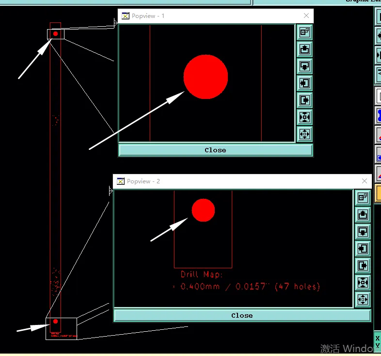
Figure 4: The aperture size of the NPTH hole at the marking is not provided
For the large 8.05 mm holes, we recommended widening routing tolerance to ±0.1 mm for better manufacturability.
Manufacturing Risks and DFM Insights
This case demonstrates the challenges of thick, narrow PCBs. High board thickness combined with small vias creates significant aspect ratio issues that affect plating and mask tenting. Lack of panelization on narrow boards increases handling risk and reduces production efficiency. Missing hole dimensions and tooling features are common oversights that force last-minute adjustments.
Designers often underestimate the mechanical difficulties of processing long, thin, thick boards without adequate support features.
How the Engineering Team Resolved the Issues
Our team created a recommended panel layout with stamp holes and added necessary tooling/fiducial holes. We provided clear markup showing via drill compensation and updated production files. After customer review and approval of the panel approach, hole tolerances, and marking positions, the manufacturing data was finalized.
To reduce manufacturing risk, we optimized the process for the high-thickness board while maintaining single-piece delivery capability after depanelization.
Final Manufacturing Outcome
All engineering questions were clarified and approved. Production files were updated with optimized panelization, via compensation, and mechanical features. The order successfully passed DFM review and moved into production.
Key Takeaways for PCB Designers
- For thick boards (>3 mm), carefully evaluate via sizes and consider drill compensation for reliable tenting and plating.
- Long, narrow boards benefit greatly from panelization or added tooling holes even if final delivery is single piece.
- Always specify hole diameters for all NPTH features and provide clear thickness tolerances.
- Include fiducials and locating holes on process edges or near board edges for accurate routing.
- Plan stamp hole or mouse-bite panelization for easier handling of awkward shapes.
- Provide production marking requirements and preferred locations early to avoid placement conflicts.
- Work with your manufacturer on DFM for high-thickness or high-aspect-ratio designs to prevent unexpected issues.
FAQ
Q1: Why is via tenting risky on thick boards with small holes?
A1: High aspect ratio makes it difficult for solder mask ink to cover the hole without flowing inside, causing blockage and potential solder bead entrapment during assembly.
Q2: Should narrow long PCBs always be panelized?
A2: Yes, for production efficiency and stability. Stamp holes allow easy separation while providing better handling during manufacturing.
Q3: What is the typical thickness tolerance for 4 mm PCBs?
A3: Per IPC standards, ±10% is commonly accepted unless tighter tolerance is specified and feasible.
Q4: Why add tooling holes even for single-piece boards?
A4: They ensure accurate registration during drilling and routing, preventing dimensional errors on long, narrow boards.
Q5: What risks come from missing NPTH hole dimensions?
A5: Manufacturers must guess sizes from outlines, which can lead to incorrect hole diameters and fitment problems in final assembly.