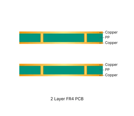
2 Layer FR4 PCB Production Record #FR4-20260314-020
| Parameter | Value | Parameter | Value |
|---|---|---|---|
| PCB Type | FR4 PCB | Quantity | 10 pcs |
| Layers | 2 Layers | Board Type | Single PCB |
| Dimensions | 570 x 20 mm | Copper Weight | 3oz |
| Thickness | 4 mm | Min Track / Spacing | 10/10mil |
| Surface Finish | HASL Lead Free | Min Hole Size | 0.5mm |
| Solder Mask | Matte Black | Silkscreen | White |
| Stack-up | Custom | Impedance Control | No |
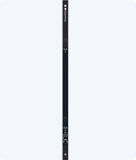
This 2-layer FR-4 board (570 × 20 mm, 4.0 mm finished thickness) was produced as 10 pieces using KB-6165F TG150 material with 1 oz / 3 oz copper. The long narrow aspect ratio required careful handling during processing. Key specifications included 0.5 mm minimum holes, 10 mil line width/space, lead-free HASL surface finish, and via tenting. Production was completed in 16 days with 100% flying probe testing, electrical test reports, and quality certificates delivered.
Given the 4 mm thickness and single-piece shipment requirement, production used a 10-up panel with stamp hole connections (0.8 mm holes at 0.25 mm spacing) for stability. Tooling holes (2.0 mm) and fiducials (1.0 mm) were added on process edges 5 mm from the board outline. The 0.4 mm vias specified for tenting were pre-drilled to 0.6 mm to reduce the risk of ink intrusion and solder bead entrapment in the high aspect ratio holes. NPTH hole size was confirmed at 8.05 mm with adjusted routing tolerance of ±0.1 mm. Thickness tolerance followed IPC ±10%, and production numbering was placed as requested.
All DFM clarifications were resolved before release, resulting in boards that met dimensional, plating, and electrical requirements with clean edges after depanelization. For detailed handling of the via tenting and panelization approach in this 4 mm thick build, refer to the related engineering case.
2 layer FR4 PCBs deliver cost-effective solutions for most electronic designs. Their simple structure enables consistent quality and efficient production cycles.
Real Engineering Queries (EQ) and DFM issues for 2 Layer FR4 PCB (double-sided boards) from actual production reviews. Learn how to avoid common problems with via treatment, silkscreen on pads, solder mask openings, hole attributes, board edge clearance, and other frequent design pitfalls.
| Order ID | PCB Type | Layers | Dimensions | Solder Mask | Surface Finish | Quantity | Action |
|---|---|---|---|---|---|---|---|
| FR4-20260630-014 | FR4 PCB | 2 | 126 x 145 | Green | ENIG (Immersion Gold) | 10 | View detail |
| FR4-20260628-010 | FR4 PCB | 2 | 60 x 120 | Green | HASL Lead Free | 5 | View detail |
| FR4-20260619-010 | FR4 PCB | 2 | 121 x 121 | Green | HASL Lead Free | 50 | View detail |


