Introduction
In high-mix, low-volume PCB assembly, production runs often involve prototypes, custom designs, or small batches that change frequently. Traditional testing methods struggle here because they demand costly custom fixtures and long setup times, which erode margins on limited quantities. Flying probe testing emerges as a compelling option for these scenarios, offering fixtureless electrical verification that aligns well with dynamic workflows. Engineers evaluating PCB assembly testing strategies frequently consider flying probe testing for small batch PCB production due to its adaptability. This approach minimizes upfront costs while delivering reliable fault detection across diverse board types. As demands for rapid iteration grow, understanding if flying probe testing truly matches high mix low volume PCB testing needs becomes essential for efficient quality control.
What Is Flying Probe Testing?
Flying probe testing uses independently controlled probes mounted on robotic arms to make electrical contact with test points on a PCB. These probes move precisely to nets defined in the board's CAD data, checking for opens, shorts, resistance values, and capacitance without physical fixtures. Typically, systems employ four to eight probes, often paired with optical vision for alignment, enabling tests on both bare boards and assembled units. This method supports in-circuit testing post-SMT assembly by verifying component presence, solder joint integrity, and basic functionality. For electric engineers, the appeal lies in its programmability, which imports netlists directly and adjusts for design variations on the fly. In essence, flying probe testing provides a versatile electrical test platform suited to non-standardized production.
Why Flying Probe Testing Excels in High-Mix, Low-Volume PCB Assembly
High-mix, low-volume environments feature frequent design changes, small quantities per variant, and tight timelines, making fixture-based tests impractical. Flying probe testing sidesteps fixture costs, which can exceed thousands per board type, allowing immediate testing upon assembly completion. FPT for HMLV shines in prototype validation and pilot runs, where flexibility trumps speed. It achieves high test coverage, often exceeding 90% of nets without mechanical constraints, crucial for complex, densely populated boards. Engineers benefit from reduced lead times, as programming takes hours rather than weeks for fixture fabrication. Overall, this positions flying probe testing small batch PCB workflows as cost-effective without sacrificing precision.
Technical Principles of Flying Probe Testing
At its core, flying probe systems rely on high-resolution motion control, with probes traveling at speeds up to several inches per second between points. Each probe tip, often spring-loaded with interchangeable ends, applies controlled force to penetrate oxides or contaminants for reliable contact. Vision cameras assist in fiducial recognition and component offset compensation, ensuring accuracy down to microns. Test algorithms perform continuity checks by sourcing current and measuring voltage drops, alongside parametric tests like resistor values or capacitor leakage. Compliance with standards such as IPC-9252 ensures these measurements meet industry benchmarks for bare board and assembly electrical testing. Multi-frequency vector measurements further detect subtle faults like weak solder joints, making the process robust for varied HMLV assemblies.
The system's software integrates Gerber, ODB++, or IPC-D-356 netlist files, automatically generating test sequences. Probe configurations adapt to board size and complexity, with top and bottom access for double-sided testing. Environmental controls, like temperature stabilization, prevent thermal expansion errors during extended runs. For assembled boards, boundary scan integration via JTAG enhances coverage where probes cannot reach. These principles collectively enable FPT to handle the variability inherent in high mix low volume PCB testing.
PCB Assembly Testing Strategies Incorporating FPT
Integrate flying probe testing early in the HMLV workflow, right after SMT reflow and selective soldering, to catch defects before final assembly. Start with bare board FPT to verify fabrication quality per IPC-6012 performance specs, then repeat post-assembly for populated verification. Optimize test programs by prioritizing critical nets, such as power rails and high-speed signals, to balance coverage and throughput. Combine with AOI for visual defects and X-ray for BGA inspection, forming a layered PCB assembly testing strategy. For small batches, batch multiple similar designs into one program to maximize machine utilization. Regularly calibrate probes and update software for evolving designs to maintain consistency.
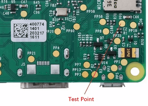
Design for testability proves vital: allocate at least 10% of copper area to accessible test points, spaced 0.5mm minimum from components. Avoid vias under parts and ensure fiducials in corners for alignment. In troubleshooting scenarios, log false calls from probe bounce on flexible traces and adjust contact force accordingly. These practices ensure FPT delivers actionable data, reducing escapes to downstream processes.
Comparing FPT with Other Testing Methods for HMLV
Bed-of-nails testers offer blazing speed for high-volume runs but falter in HMLV due to fixture NRE costs and inflexibility for revisions. Flying probe testing, conversely, scales effortlessly to new designs without hardware changes. Functional testing verifies end-use performance but misses isolated faults; FPT complements it by providing granular electrical data pre-function. Boundary scan suits digital-heavy boards but requires embedded test logic, unlike probe's universal access. In cost-benefit analysis for prototypes, FPT often undercuts alternatives by 50-70% in setup expenses, though throughput lags for volumes over 100 units.
- Bed-of-Nails — Best for: High-volume; HMLV suitability: Low (fixture cost); Key trade-offs: Fast, but rigid.
- Flying Probe — Best for: Prototypes and HMLV; HMLV suitability: High; Key trade-offs: Flexible, slower.
- Functional — Best for: Final validation; HMLV suitability: Medium; Key trade-offs: Comprehensive, time-intensive.
- Boundary Scan — Best for: Digital ICs; HMLV suitability: Medium; Key trade-offs: Logic-dependent.
This list highlights why FPT for HMLV dominates small batch scenarios.
Troubleshooting Common Issues in Flying Probe Testing for Small Batch PCBs
Probe misalignment tops common pitfalls, often from fiducial misalignment or board warpage; counter it with multi-camera vision and orthogonal probing. Access denied errors arise on BGA or fine-pitch parts, resolved by adding bed-of-nails hybrids for hybrids or redesigning test pads. False opens from poor contact on gold-plated pads demand tip cleaning cycles and force optimization. High capacitance boards slow testing; mitigate via frequency sweeps per IPC guidelines. Log parametric drifts to trace assembly variances like cold joints. Systematic review of failure modes refines programs, boosting first-pass yields in variable HMLV runs.
Component tolerance variations trigger out-of-spec calls; baseline golden boards to set limits dynamically. Environmental factors, such as humidity-induced leakage, require preconditioning. These targeted fixes ensure reliable high mix low volume PCB testing outcomes.
Conclusion
Flying probe testing proves a near-perfect match for high-mix, low-volume PCB assembly, balancing flexibility, cost, and coverage where rigid methods fail. Its fixtureless nature empowers rapid prototyping and small batch validation, aligning with modern agile engineering demands. By adhering to best practices and standards like IPC-9252, teams achieve robust quality without volume-scale investments. For electric engineers refining PCB assembly testing strategies, FPT stands out as a practical cornerstone. Embracing it enhances reliability while streamlining workflows in dynamic production landscapes.
FAQs
Q1: What makes flying probe testing ideal for small batch PCB production?
A1: Flying probe testing eliminates custom fixtures, slashing setup costs for prototypes and low volumes. It offers high flexibility for design changes common in HMLV, with programmable probes accessing diverse nets quickly. Test coverage rivals fixed systems, detecting shorts and opens reliably. This makes it a go-to for efficient flying probe testing small batch PCB runs without compromising quality.
Q2: How does FPT fit into high mix low volume PCB testing strategies?
A2: FPT integrates seamlessly post-SMΤ, verifying assembly integrity before functional tests. Its CAD-driven programming handles mix variability, reducing programming time per variant. Combine with AOI for comprehensive coverage. Engineers gain troubleshooting insights from detailed logs, optimizing future iterations in high mix low volume PCB testing.
Q3: What are key best practices for FPT in HMLV assembly?
A3: Prioritize accessible test points and fiducials in design. Calibrate probes regularly and baseline with known-good boards. Segment tests for critical nets first to shorten cycles. Monitor environmental factors to avoid false calls. These steps maximize throughput and accuracy in FPT for HMLV applications.
Q4: Can flying probe testing meet IPC standards for PCB electrical testing?
A4: Yes, FPT complies with IPC-9252 requirements for continuity and isolation tests on bare and assembled boards. It supports parametric measurements aligned with performance specs. Proper programming ensures Level B or C coverage, vital for reliable HMLV production.
References
IPC-9252 — Electrical Test of Bare Printed Wiring Boards. IPC
IPC-6012E — Qualification and Performance Specification for Rigid Printed Boards. IPC, 2017
J-STD-001H — Requirements for Soldered Electrical and Electronic Assemblies. IPC, 2018


