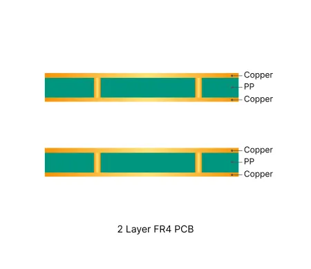
2 Layer FR4 PCB Production Record #FR4-20260423-049
| Parameter | Value | Parameter | Value |
|---|---|---|---|
| PCB Type | FR4 PCB | Quantity | 20 pcs |
| Layers | 2 Layers | Board Type | Panel PCB |
| Dimensions | 179 x 158.3 mm | Copper Weight | 1oz |
| Thickness | 1.6 mm | Min Track / Spacing | 3/3mil |
| Surface Finish | ENIG (Immersion Gold) | Min Hole Size | 0.3mm↑ |
| Solder Mask | Green | Silkscreen | White |
| Stack-up | Custom | Impedance Control | No |
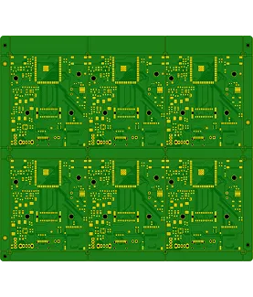
This 2-layer FR-4 board (179 × 158.3 mm, 1.6 mm finished thickness) was produced in a quantity of 120 pieces (20 sets) on KB-6165F TG150 material with 1 oz copper on both sides. The design featured 0.3 mm minimum holes, 3 mil line width/space, ENIG surface finish, full solder mask over vias, and 3×2 panelization with 7 mm process edges on all four sides using V-CUT depanelization. Production was completed in 11 days with 100% flying probe testing and delivery of electrical test reports plus quality certificates.
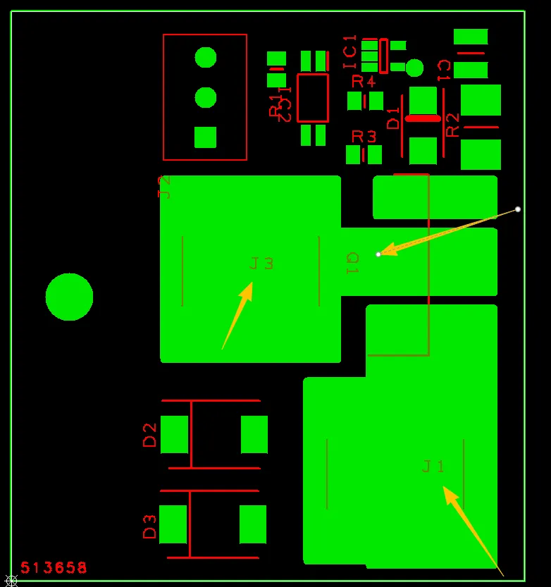
DFM review focused on panelization and manufacturability. Component pads positioned too close to or over the board edge were adjusted per customer panel design recommendation to maintain 7 mm borders and prevent exposed copper. Tight 4 mil pad spacing was highlighted as insufficient for reliable solder mask bridges; customer confirmation was obtained on acceptable minimums. PTH holes without solder mask openings risked ink flow onto pads affecting component insertion, while mixed via windowing (some double-sided open) required clarification to avoid ink intrusion and edge redness. Silk screen frames, character placement near pads, and process edge details including fiducials, V-CUT lines, and copper balancing were all verified and optimized in the final production files.
All confirmed adjustments were implemented, resulting in boards that met dimensional tolerances, solder mask coverage, and electrical requirements with clean V-CUT edges. For detailed resolution of the tight pad spacing and edge clearance along with V-CUT panelization handling in this build, refer to the related engineering case.
2 layer FR4 PCBs deliver cost-effective solutions for most electronic designs. Their simple structure enables consistent quality and efficient production cycles.
Real Engineering Queries (EQ) and DFM issues for 2 Layer FR4 PCB (double-sided boards) from actual production reviews. Learn how to avoid common problems with via treatment, silkscreen on pads, solder mask openings, hole attributes, board edge clearance, and other frequent design pitfalls.
| Order ID | PCB Type | Layers | Dimensions | Solder Mask | Surface Finish | Quantity | Action |
|---|---|---|---|---|---|---|---|
| FR4-20260528-028 | FR4 PCB | 2 | 185 x 245 | Green | HASL Lead Free | 5 | View detail |
| FR4-20260526-001 | FR4 PCB | 2 | 100 x 100 | Green | HASL Lead Free | 10 | View detail |
| FR4-20260525-001 | FR4 PCB | 2 | 50 x 45 | Matte Green | HASL Lead Free | 20 | View detail |


