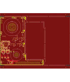
ENIG FR4 PCB Production Record #FR4-20260327-031
| Parameter | Value | Parameter | Value |
|---|---|---|---|
| PCB Type | FR4 PCB | Quantity | 5 pcs |
| Layers | 18 Layers | Board Type | Panel PCB |
| Dimensions | 235.55 x 187 mm | Copper Weight | 0.5oz |
| Thickness | 2 mm | Min Track / Spacing | 3/3mil |
| Surface Finish | ENIG (Immersion Gold) | Min Hole Size | 0.2mm |
| Solder Mask | Red | Silkscreen | White |
| Stack-up | Custom | Impedance Control | Yes |
This 18-layer FR-4 board (235.55 × 187 mm, 2.0 mm finished thickness) was built on Shengyi S1000-2M TG170 material using 0.5 oz copper on inner and outer layers. Production involved standard 1×2 panelization with customer-supplied panels, ENIG surface finish, and full impedance control. A total of 10 pieces (5 sets) were delivered after 21 days, with electrical testing and quality documentation provided. Key features included 0.2 mm minimum hole size, resin plugging of vias, and selective back-drilling.
During DFM review, large copper-void areas on inner layers were identified as a lamination risk that could cause wrinkling or delamination under press. These were addressed through copper balancing adjustments prior to production. Impedance requirements led to substitution with high-speed R5775G material, followed by stack-up and trace width compensation to match target values based on provided data and available core/prepreg inventory. Back-drill locations at positions 18-15 and similar vias were clarified and standardized in the production files to maintain registration consistency. Resin plugging specifications required careful solder mask window management to avoid ink encroachment on BGA pads while ensuring reliable via fill.
All engineering changes, including serial number, logo, and QR code marking, were implemented after file confirmation. The completed boards met impedance, electrical, and dimensional requirements with no reported issues in final testing. For further details on the impedance-controlled stack-up and back-drill registration management, refer to the related engineering case.
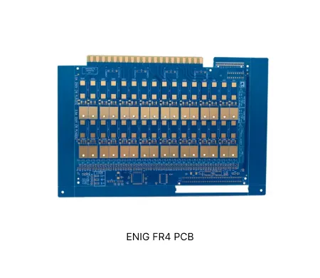
FR4 material with ENIG finish provides balanced electrical performance, shelf life, and assembly compatibility for industrial and high-reliability electronics.
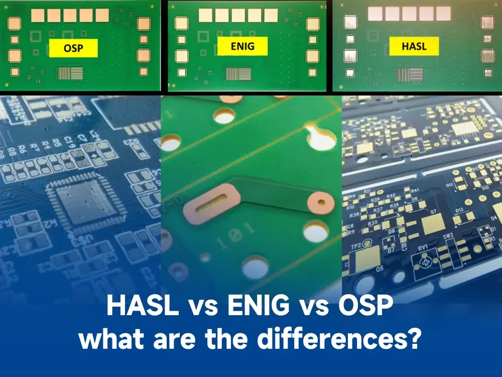
Explore common engineering queries in ENIG, HASL, and OSP FR4 PCBs. Learn real DFM challenges, surface finish compatibility issues, and practical solutions to reduce manufacturing risks and improve yield.
| Order ID | PCB Type | Layers | Dimensions | Solder Mask | Surface Finish | Quantity | Action |
|---|---|---|---|---|---|---|---|
| FR4-20260630-014 | FR4 PCB | 2 | 126 x 145 | Green | ENIG (Immersion Gold) | 10 | View detail |
| FR4-20260529-059 | FR4 PCB | 2 | 147.3 x 53.8 | Green | ENIG (Immersion Gold) | 5 | View detail |
| FR4-20260520-046 | FR4 PCB | 2 | 94.21 x 275 | Green | ENIG (Immersion Gold) | 75 | View detail |


