This engineering case study examines a real 8-layer PCB order that underwent detailed CAM review at our facility. The board features a 170×270mm outline, 1.6mm finished thickness, mixed 0.5/1oz copper, ENIG surface finish, and blind vias. While the design appeared standard on paper, the CAM engineering team identified several manufacturability issues that required customer clarification before production release.
8-layer boards with blind vias and specific panelization requirements frequently trigger engineering questions (EQs) because design intent often conflicts with actual fabrication capabilities. In this case, our CAM review prevented potential production delays and quality risks. We share the key findings here to help designers understand common DFM pitfalls in multilayer fabrication.
Order Overview
This was a 30-piece (30 sets) order of 8-layer FR-4 TG170 boards (#FR4-20260205-046). Finished thickness was specified at 1.6mm with 0.5oz inner and 1oz outer copper. Minimum hole size was 0.3mm, and the design included blind vias. The customer requested 100% flying probe testing, ENIG surface finish, and client self-panelization with 3-up array. Delivery was set for 12 days.
The stackup involved multiple core boards, which immediately raised concerns during material planning. Solder mask was green on both sides, silkscreen white, and the design included slotted holes and specific mechanical features. While the overall parameters fell within our standard capabilities for FR-4 material, several details in the fabrication data required clarification to ensure reliable yield.
Main Engineering Questions Identified During CAM Review
1. Stackup Optimization for 8-Layer FR4 TG170 PCB: Multiple Cores vs. Feasibility
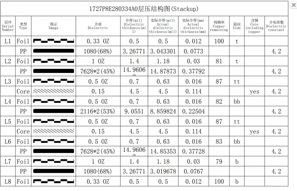
The original customer stackup called for three core boards, which significantly increased material cost and complexity. We noticed that the specified 0.4mm cores were not readily available in our inventory for this run. After internal review, our engineering team adjusted the PP (prepreg) and core thicknesses while maintaining the target 1.6mm finished board thickness and impedance requirements where possible.
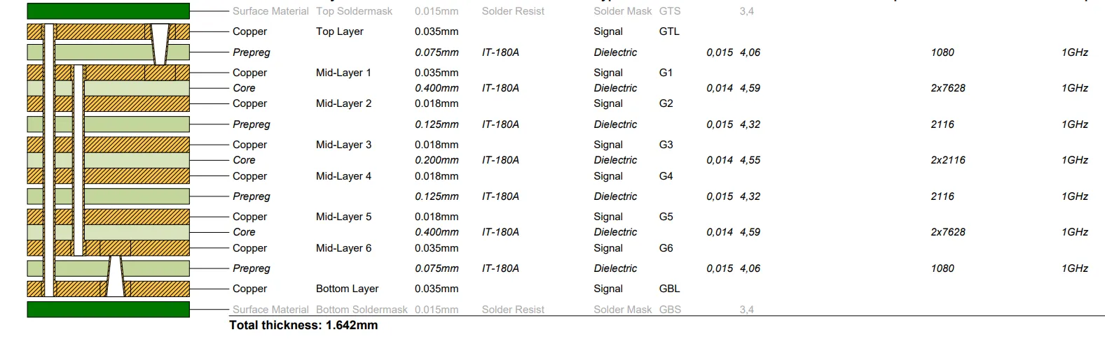
Figure 1: Original customer stackup
We sent the revised lamination diagram for confirmation. Our engineer suggested this change because using three cores would have driven up both cost and lamination risk, including potential delamination or warpage due to increased resin flow variation. If ignored, the board could have suffered from inconsistent thickness across the panel or resin voids between layers, leading to reliability issues in subsequent assembly and thermal cycling.
Figure
| Aspect | Original Customer Stackup | Revised Manufacturing Stackup | Benefit |
|---|---|---|---|
| Core Configuration | Three 0.4mm cores | Adjusted PP + core thicknesses | Reduced cost and lamination risk |
| Finished Thickness | 1.6mm | 1.6mm (maintained) | Consistent impedance and flatness |
| Key Risk if Unchanged | Higher warpage/delamination potential | Lower resin flow variation | Improved yield and reliability |
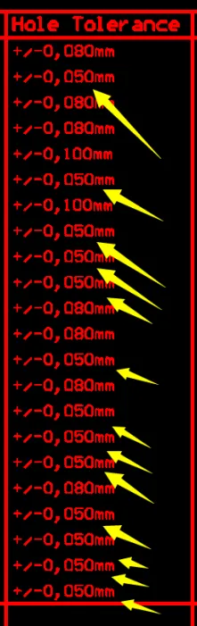
2. Board Thickness Mismatch and Tight Slot Hole Tolerances in TG170 PCB
During CAM review, we found that the customer-specified board thickness conflicted with the actual stackup calculation. Additionally, arrow-marked slotted holes had tolerances that were too tight for standard mechanical routing capabilities.
Our CAM engineer confirmed that achieving the exact slot tolerances as drawn would be challenging without secondary operations, which would increase cost and risk of burrs or breakout. We proposed standard achievable tolerances and asked for confirmation. Had production proceeded without adjustment, slot holes could have shown irregular edges or copper breakout, potentially causing assembly misalignment or short circuits at the edges.
Figure
| Feature | Customer Specification | Recommended Achievable Tolerance | Potential Risk if Too Tight |
|---|---|---|---|
| Slotted Holes | Arrow-marked tight | Standard mechanical routing | Burrs, breakout, added cost |
3. Panelization Alignment Issues: Stamp Holes and Bridge Tabs in 8-Layer PCB
The customer-provided panelization (3-up) showed misalignment between stamp holes (mouse bites) and the bridging tabs. We noticed this discrepancy during the depanelization process simulation. Our engineer highlighted the positions and requested confirmation on preferred alignment to avoid stress concentration during breaking.
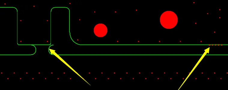
Figure 4: Misalignment between stamp holes (mouse bites) and the bridging tabs
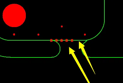
Figure 5: Detailed stamp holes and bridge positions mismatch
If left unaddressed, misaligned stamp holes could result in rough edges after depanelization, fiber tear-out, or even damage to nearby traces, especially problematic for a board with blind vias near the panel edges. This is a common issue in client self-panelized designs that we frequently see in 8-layer PCB builds.
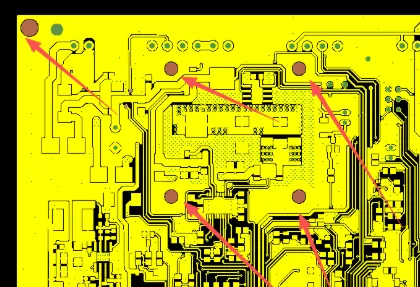
4. Undocumented Impedance Lines and Solder Mask Issues in FR4 TG170 Design
Highlighted traces appeared to be impedance-controlled lines, but the fabrication data lacked any impedance specifications or reference layers. We also identified missing silkscreen data despite customer requirements for white characters, and certain solder mask annotations that our team proposed to delete to prevent printing defects.
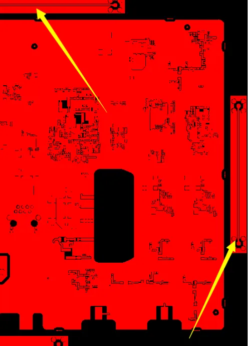
Figure 6: Impedance lines without documentation
Our CAM team identified these conflicts early. Without clear impedance requirements, we could not guarantee the target values during production. For the solder mask text, deletion was recommended because non-functional markings can cause ink bleeding or mask adhesion issues during ENIG processing. Ignoring this could lead to cosmetic defects or, worse, mask residue affecting solderability.
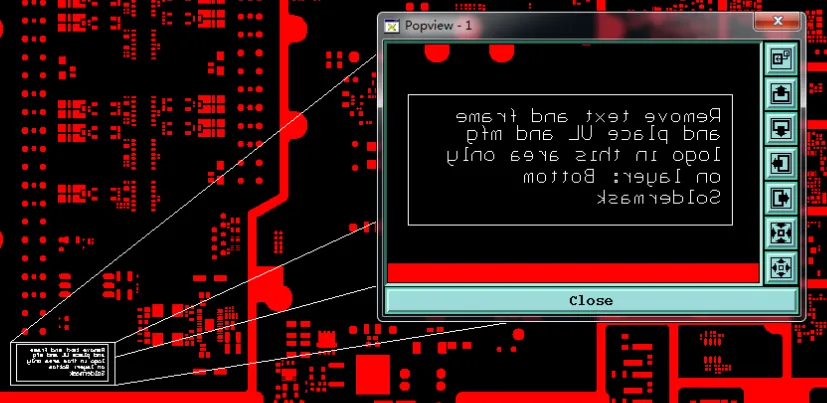
Figure 7: Deletion of non-functional markings
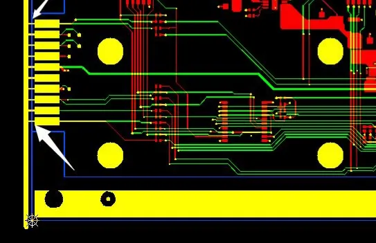
5. Process Edge Copper and Exposed Copper Risks in Multilayer PCB Panelization
To ensure production quality and plating uniformity, our team added copper to the process edges. We also planned exposed copper with potential burrs at specific attachment locations and asked for confirmation. Additionally, concentric circle features and certain highlighted regions required clarification on fabrication intent.
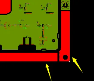
Figure 8: Edge copper pour
We noticed the V-CUT or scoring area proximity to exposed copper. Our engineer suggested adjustments because, per common IPC-A-600 considerations, insufficient clearance in these zones can lead to exposed copper after depanelization, increasing the risk of edge shorting during assembly or handling.
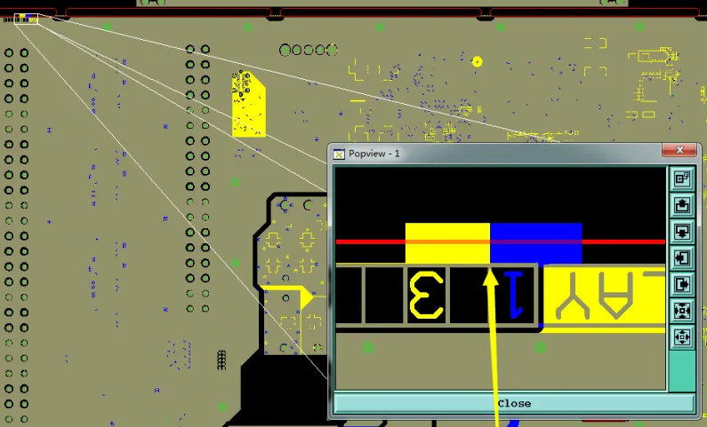
Figure 9: Exposed copper at attachment points
Manufacturing Risks and DFM Lessons from This 8-Layer FR4 TG170 Case
This case highlights several recurring DFM challenges in 8-layer designs: overly complex stackups, undocumented impedance requirements, and panelization details left to fabrication assumptions. Customers often focus on electrical performance but overlook how material availability and process tolerances affect the final product.
If the stackup had not been optimized, higher costs and increased risk of rigid PCB failures like warpage or delamination could have occurred. Tight slot tolerances without clarification frequently result in yield loss from mechanical breakout. Misaligned panel features can cause cosmetic and functional defects post-depanelization, while missing impedance specs force conservative manufacturing that may not meet design targets.
These issues demonstrate why factories raise EQs — to align design intent with manufacturing reality and avoid scrap boards or field failures.
How the Engineering Team Resolved the Issues
Our team provided a revised lamination diagram, proposed achievable tolerances for slots, and suggested alignment corrections for stamp holes. We added necessary production numbering and factory marks after confirmation. For impedance, we requested target values and reference layers. All solder mask and silkscreen clarifications were resolved by deleting non-functional elements and confirming thickness requirements.
After receiving customer approvals on the adjusted stackup and panelization, the ODB files were reprocessed successfully. Minor layer naming issues (such as gm11) were clarified and corrected in the working data.
Final Manufacturing Outcome
All engineering questions were resolved through clear communication. The stackup was optimized, panelization corrected, and fabrication data finalized. The order was approved for production with updated parameters that balanced customer requirements with reliable manufacturability. The boards proceeded to lamination, drilling, plating, and testing under controlled conditions.
Key Takeaways for PCB Designers
- Provide complete stackup drawings with core and prepreg thicknesses clearly specified. Avoid assuming factory will always have exact core sizes on hand.
- Document impedance requirements including target values, trace widths, and reference layers in fabrication notes or a separate drawing.
- Define realistic mechanical tolerances for slotted holes and other non-plated features. Consult with your manufacturer early for tight tolerance needs.
- Ensure panelization files show clear alignment between mouse bites, bridges, and board outlines. Provide breakaway tab preferences.
- Include all silkscreen and solder mask layers in the fabrication data. Clearly indicate if specific text or markings should be omitted.
- Verify ODB or Gerber files open correctly before submission and use consistent layer naming conventions.
- Consider process edge requirements and copper balancing for better plating uniformity and reduced warpage.
- Review DFM reports promptly — early clarification prevents costly revisions later in the production cycle.
FAQ
Q1: Why is stackup optimization often necessary for multilayer TG170 PCBs?
A1: Factories maintain standard core and prepreg inventories for efficiency and cost control. Custom or multiple thin cores increase material cost and lamination complexity, potentially leading to thickness variation or delamination if not adjusted to available materials.
Q2: What risks arise from undocumented impedance lines?
A2: Without specifications, the manufacturer cannot verify or tune the design. This may result in out-of-spec impedance, signal integrity issues, or the need for multiple prototyping iterations.
Q3: Why do factories adjust panelization features like stamp holes?
A3: Misalignment can cause stress during depanelization, leading to fiber tear, rough edges, or damage to copper features near the panel border. Proper alignment improves both yield and cosmetic quality.
Q4: Can slotted holes have very tight tolerances?
A4: Mechanical routing has practical limits. Extremely tight tolerances often require special processes that increase cost and risk of defects such as burrs or breakout. Designers should confirm achievable tolerances with the manufacturer.
Q5: Why add copper to process edges?
A5: Additional copper improves plating current distribution and helps maintain panel flatness during processing, reducing the risk of warpage and ensuring consistent copper thickness across the production panel.
Q6: What should designers do when receiving EQs from the factory?
A6: Respond promptly with clear references to the provided images or diagrams. Provide the requested confirmation or preferred alternatives. Early collaboration minimizes production delays and improves final board quality.