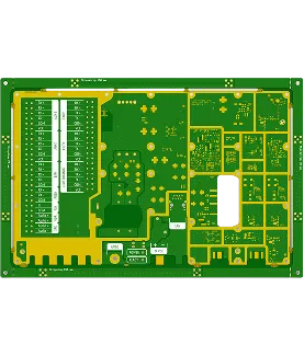
8 Layer FR4 PCB Production Record #FR4-20260205-046
| Parameter | Value | Parameter | Value |
|---|---|---|---|
| PCB Type | FR4 PCB | Quantity | 30 pcs |
| Layers | 8 Layers | Board Type | Panel PCB |
| Dimensions | 170 x 270 mm | Copper Weight | 1oz |
| Thickness | 1.6 mm | Min Track / Spacing | 6/6mil↑ |
| Surface Finish | ENIG (Immersion Gold) | Min Hole Size | 0.3mm↑ |
| Solder Mask | Green | Silkscreen | White |
| Stack-up | Custom | Impedance Control | No |
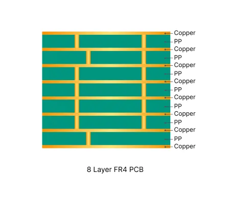
This 8-layer FR-4 TG170 PCB (170 × 270 mm, 1.6 mm finished thickness) was produced in a 3-panel array for a total of 30 pieces. Inner layers used 0.5 oz copper and outer layers 1 oz, with 0.3 mm minimum holes, 6 mil trace/space, and ENIG surface finish. The stackup was adjusted during CAM review after confirming material availability—no 0.4 mm cores were in stock—so PP and core thicknesses were optimized to maintain overall thickness and impedance stability while controlling press parameters.
Multiple DFM issues were resolved prior to production. Panelization alignment between stamp holes and bridges was corrected to prevent misalignment during routing. Slot and plated hole tolerances were tightened where possible while respecting mechanical limits; non-plated holes were fabricated as specified. Solder mask clearance, legend placement (including added production numbering and factory marks), and process-edge copper balancing were finalized after customer confirmation. ODB file discrepancies and missing layer data (e.g., GM11) were clarified and corrected in the working gerber set.
The stackup optimization and panelization alignment decisions ensured reliable lamination and consistent board thickness. All boards passed 100% electrical testing with no rework required. The order was completed within the 12-day lead time and shipped as planned.
These multilayer boards support dense circuitry with eight copper layers while maintaining controlled impedance and thermal performance.

In-depth guide to the most frequent Engineering Queries (EQ) and DFM issues in Multilayer FR4 PCB (4/6/8+ layers) production. Real factory insights on stack-up confirmation, impedance control, copper balance, inner layer design, via treatment, registration, and practical prevention strategies.
| Order ID | PCB Type | Layers | Dimensions | Solder Mask | Surface Finish | Quantity | Action |
|---|---|---|---|---|---|---|---|
| FR4-20260630-014 | FR4 PCB | 2 | 126 x 145 | Green | ENIG (Immersion Gold) | 10 | View detail |
| FR4-20260529-059 | FR4 PCB | 2 | 147.3 x 53.8 | Green | ENIG (Immersion Gold) | 5 | View detail |
| FR4-20260520-046 | FR4 PCB | 2 | 94.21 x 275 | Green | ENIG (Immersion Gold) | 75 | View detail |


