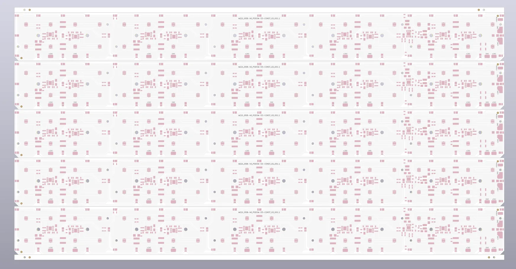
Introduction
In actual production of aluminum substrate PCBs, surface finish selection plays a critical role in both thermal performance and assembly reliability. HASL and OSP are two common options, yet each brings distinct interactions with the aluminum base and dielectric layer that frequently generate engineering queries during file review. Factory teams often see designs where the chosen finish conflicts with pad geometry, thermal via configurations, or overall board flatness requirements. These queries arise because aluminum PCBs are engineered primarily for heat dissipation in applications like LED lighting and power modules, making standard FR4 practices insufficient. Clarifying these points early helps prevent defects such as uneven coating, poor solderability, or delamination risks during lamination and finishing processes.
Engineering queries (EQs) serve as essential communication between design teams and manufacturers. For HASL Aluminum PCB and OSP Aluminum PCB, they typically focus on how the surface finish process affects the metal core's thermal properties and the thin dielectric layer's integrity. In our experience, unresolved questions around finish compatibility can delay panelization decisions and impact final yield. Addressing them proactively ensures the board meets both electrical and thermal expectations without introducing process-induced stresses.
What Are Engineering Queries and Why They Matter for HASL Aluminum PCB and OSP Aluminum PCB
Engineering queries are clarification requests issued by the CAM or DFM engineering team when Gerber, drill, or stack-up data contains ambiguities that could lead to manufacturing defects. In HASL Aluminum PCB and OSP Aluminum PCB production, these queries matter because the aluminum core introduces unique thermal expansion behavior and bonding challenges with the dielectric. A single unclear specification on surface finish application can affect solder mask adhesion, copper pad protection, or overall board flatness. Factory observations show that timely responses to EQs reduce scrap rates and ensure the finished boards deliver the expected heat dissipation performance. Without them, production may proceed with assumptions that compromise reliability in high-power environments.
Common EQ Types for HASL Aluminum PCB and OSP Aluminum PCB
One frequent EQ concerns compatibility of HASL with aluminum substrate thermal vias or exposed areas. Designers sometimes specify HASL on boards with dense thermal via arrays or minimal solder mask coverage near the aluminum edge, assuming uniform solder flow. This occurs because HASL involves hot air leveling after solder application, which can transmit thermal shock through the thin dielectric to the aluminum core, potentially causing uneven expansion or micro-cracks if via plating and copper balance are not optimized. During engineering review, the DFM check flags potential bridging on fine pads or incomplete leveling due to the board's thermal mass, triggering a request for confirmation on via tenting or exposed aluminum zones. If left unclarified, the risk includes solder bridging, poor flatness affecting SMT assembly, or reduced thermal conductivity from process-induced stresses.
Another common query involves OSP application on aluminum PCBs with large copper pours or mixed pad sizes. The organic coating is thin and transparent, leading designers to overlook how surface preparation on the copper side interacts with the aluminum bonding process. The root cause often lies in incomplete stack-up notes or missing specifications for OSP thickness and multiple reflow expectations, as OSP has limited thermal cycle durability. In file review, CAM engineers detect this through solder mask clearance checks and surface finish callouts, requesting clarification on pad exposure and handling instructions. Without resolution, potential defects include uneven coating leading to oxidation, inconsistent solder wetting during assembly, or premature degradation in humid environments, ultimately affecting long-term reliability of the heat-dissipating board.
Solder mask registration and overlap on HASL-finished aluminum PCBs also trigger frequent EQs, particularly when designs feature tight tolerances around thermal pads. The issue appears when solder mask openings do not adequately account for the slight surface variation introduced by HASL leveling combined with aluminum's rigidity. This stems from design files lacking explicit notes on mask expansion or dielectric thickness variations. Detection happens via automated DFM tools that compare mask layers against copper and drill data, prompting questions about minimum web width or intentional exposure. If ignored, risks include mask encroachment on pads causing solderability issues or insufficient coverage leading to copper oxidation and potential shorts in high-voltage applications.
Panelization and routing for OSP Aluminum PCB designs often raise queries related to dimensional stability. Aluminum cores expand differently from the circuit layers, and OSP's sensitivity to handling can compound stresses during depanelization if V-scoring or tab routing is not clearly defined. The cause is usually ambiguous panel drawings or missing notes on breakaway tab placement relative to thermal vias. Engineering review identifies this through panel layout analysis and requests confirmation on routing method to avoid damaging the fragile OSP layer or dielectric bond. Unresolved, this can result in board warpage, cracked vias, or compromised solderability on the final separated boards.
Why These EQ Occur During File Review
These engineering queries surface during file review because aluminum PCBs combine a rigid metal core with a thin dielectric and standard copper circuitry, creating process interactions not present in conventional FR4 boards. Surface finishes like HASL introduce thermal and mechanical stresses, while OSP demands precise handling and limited exposure, both of which require explicit data that many design packages do not fully capture by default. Factory DFM checks compare the provided Gerber files, drill attributes, and stack-up against equipment capabilities for lamination, drilling, plating, and finishing. Ambiguities in via intent, copper distribution, or finish-specific notes force clarification to prevent downstream defects. In practice, these questions protect yield by aligning the design with real production constraints before committing to panels.
Practical Solutions and Best Practices to Minimize EQ
To minimize EQs, provide a detailed stack-up drawing that clearly specifies aluminum base thickness, dielectric material and thickness, copper weights, and the exact surface finish with any special requirements. Include notes on expected operating temperature, thermal via plating status (plated or non-plated), and whether vias should be tented or filled. For HASL, maintain adequate pad spacing to accommodate potential unevenness and avoid fine-pitch components where possible. For OSP, define handling and storage instructions and limit designs to applications with fewer reflow cycles.
Balance copper distribution across layers as evenly as practical to reduce warpage risk during lamination and finishing. Use symmetric designs where feasible and add non-functional copper where it does not affect electrical performance. Specify solder mask color, type, and minimum overlap on pads, along with precise clearances for any exposed aluminum areas. In panelization, clearly define V-score depth, tab routing locations, and fiducial placements to ensure stability during processing. Submitting these details upfront allows the factory to validate against capabilities and reduces back-and-forth during review.
Conclusion
HASL Aluminum PCB and OSP Aluminum PCB designs demand careful attention to surface finish interactions with the metal core and dielectric to achieve reliable thermal performance. By understanding common engineering queries around compatibility, registration, and process stresses, designers can deliver cleaner files that move smoothly through production. Factory experience shows that proactive DFM alignment significantly lowers risks of defects and shortens overall lead times. Incorporating clear documentation and balanced layouts from the start benefits both manufacturability and end-product reliability in heat-sensitive applications.
FAQs
Q1: Can HASL be reliably applied to aluminum PCBs with dense thermal vias?
A1: HASL is possible but requires careful via design and copper balancing to manage thermal shock during leveling. Factory teams often request confirmation on via tenting or filling to prevent uneven surfaces or stress on the dielectric. Proper specification helps maintain flatness and solderability without compromising heat dissipation.
Q2: Why does OSP on aluminum PCBs sometimes trigger questions about shelf life and handling?
A2: OSP is a thin organic coating sensitive to oxidation and mechanical damage, with shorter durability compared to metallic finishes. On aluminum substrates, additional queries arise regarding storage conditions and multiple reflow compatibility due to the core's thermal mass. Clear notes on expected usage environment help the factory recommend adjustments if needed.
Q3: How important is copper balance in HASL or OSP aluminum PCB designs?
A3: Copper balance is critical to minimize warpage caused by CTE differences between aluminum, dielectric, and copper during lamination and surface finishing. Imbalance can exacerbate issues during HASL thermal exposure or OSP application. Designers should aim for symmetry and consider adding balancing elements where electrically feasible.
Q4: What solder mask considerations are unique to aluminum PCBs with these finishes?
A4: Solder mask must provide adequate overlap on pads while accounting for any surface variation from HASL or the thin nature of OSP. Queries often focus on web width and registration to prevent encroachment or insufficient protection. Specifying type, color, and clearances clearly reduces risks of solderability or oxidation issues.
References
IPC-6012E — Qualification and Performance Specification for Rigid Printed Boards. IPC, 2017
IPC-6013D — Qualification and Performance Specification for Flexible Printed Boards. IPC, 2019
IPC-A-600H — Acceptability of Printed Boards. IPC, 2020