Introduction
In actual production, Heavy Copper FR4 PCBs are widely used in power electronics, automotive systems, and high-current applications where standard copper weights cannot meet thermal and current-carrying demands. Factory teams frequently observe that these boards introduce unique challenges during engineering review compared to standard FR4 designs. The thicker copper layers affect etching, lamination, drilling, and plating processes in ways that often require clarification from the designer. Understanding these common engineering queries helps designers submit cleaner files and reduces delays in manufacturing.
Engineering queries arise because heavy copper demands tighter process controls and specific adjustments that may not be evident from the design files alone. In our experience, unresolved issues can lead to defects such as uneven trace profiles, layer misalignment, or reliability concerns under thermal cycling. By addressing typical questions early, both design and procurement teams can achieve smoother production runs and higher first-pass yields.
What Are Engineering Queries and Why They Matter for Heavy Copper FR4 PCB
Engineering queries, or EQs, are formal requests from the fabrication team for clarification or correction when design files contain ambiguities, conflicts, or features that risk manufacturing defects. For Heavy Copper FR4 PCB, these queries become more frequent due to the interaction between thick copper foils and standard FR4 processes. They matter because heavy copper boards are often deployed in demanding environments where reliability is critical, and small process variations can amplify into field failures. In production, an unresolved EQ can halt panelization or require costly re-engineering of the stackup and tooling.
Factory DFM reviews focus on ensuring the design is compatible with etching chemistry, lamination pressures, and plating current densities specific to thicker copper. Prompt responses to EQs prevent issues like incomplete etching or delamination, which are harder and more expensive to fix after lamination. For procurement teams, minimizing EQs shortens lead times and reduces the risk of receiving boards that fail electrical or thermal testing.
Common EQ Types for Heavy Copper FR4 PCB
One frequent EQ concerns copper imbalance and potential warpage. Designers often submit stackups with heavy copper on outer layers only or with significantly different copper densities between layers, creating uneven thermal expansion during lamination. This happens because the coefficient of thermal expansion differs markedly between thick copper and FR4 dielectric, especially when copper distribution is asymmetric. During engineering review, CAM software flags high risk of bow and twist, prompting a clarification request on acceptable warpage tolerance or proposed balancing techniques such as copper thieving. If not clarified, the risk includes boards exceeding flatness specifications, leading to assembly misalignment or reliability failures under thermal cycling.
Another common query involves etching challenges with thick copper features. When files specify fine traces or tight spacing alongside heavy copper weights, the etchant undercuts or leaves rough sidewalls because thicker foil requires longer etch times. The root cause is usually insufficient compensation in the design data or lack of specification for etch factor. In DFM checks, engineers detect this through trace width analysis and request confirmation of minimum acceptable trace width after etching or adjusted artwork. Without resolution, finished boards may have inconsistent impedance, reduced current capacity, or shorts from copper slivers.
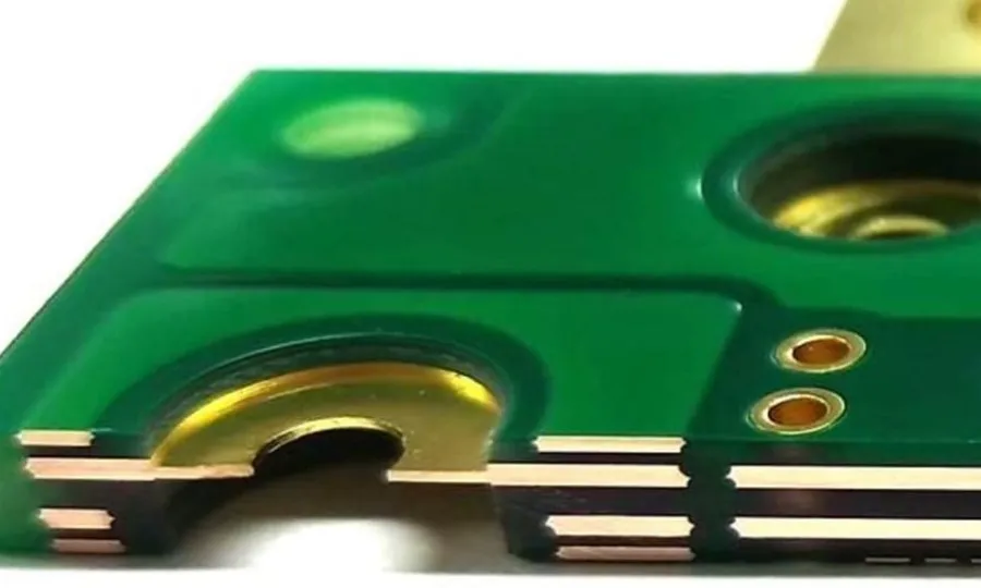
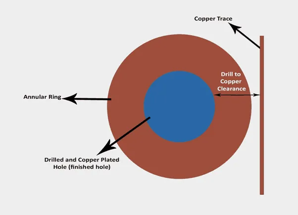
Plating uniformity in vias and through holes also triggers frequent EQs. Heavy copper outer layers combined with standard or high aspect ratio holes can result in uneven copper deposition inside the barrel due to current crowding effects. This issue stems from unspecified plating thickness requirements or via structures not optimized for the total board thickness and copper weight. CAM review highlights potential thin spots in hole walls, leading to a query for minimum plated copper thickness or via fill preferences. If left unaddressed, the board risks via cracking or open circuits during thermal stress testing, compromising long-term reliability in power applications.
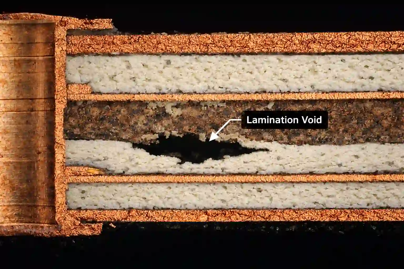
Delamination risks due to lamination parameters form another typical query. Thick copper increases mechanical stress during pressing, and mismatched dielectric thicknesses or inadequate resin flow can create voids or weak bonding at copper-dielectric interfaces. Designers sometimes provide stackups without full dielectric details or thermal relief specifications for large copper areas. Engineering teams detect this via stackup simulation and request confirmation of lamination cycle compatibility or adjustments to prepreg types. Unresolved, this can cause interlayer separation in the field, especially under repeated power cycling. Balancing copper distribution is critical—see our detailed guide on heavy copper PCB design principles, rules, and best practices.
Why These EQ Occur During File Review
These engineering queries surface because heavy copper fundamentally alters standard PCB fabrication windows. Standard FR4 processes are optimized for 1 oz or 2 oz copper, while heavy copper requires modified etching, plating, and lamination parameters that depend heavily on exact copper weights, distribution, and stackup symmetry. Design files often lack explicit notes on copper thickness per layer, etch compensation, or warpage tolerances, forcing the fabrication engineer to seek clarification to avoid process failures. In many cases, the CAD data appears manufacturable on the surface, but CAM analysis reveals interactions that only become apparent when simulating the full production sequence.
File review also catches mismatches between designer intent and factory capabilities, such as via aspect ratios that become problematic with thicker total copper. Without clear documentation, assumptions can lead to defects that only appear after costly lamination or testing. Experience shows that proactive communication during EQ resolution prevents these issues and builds better long-term design practices for heavy copper projects.
Practical Solutions and Best Practices to Minimize EQ
To reduce engineering queries, clearly specify copper weight for every layer in the fabrication notes and include a detailed stackup drawing with dielectric thicknesses and materials. Balance copper distribution as evenly as possible across layers, using copper thieving patterns where large open areas exist to minimize warpage risk. Provide minimum trace width and spacing requirements after etching compensation, and indicate any areas requiring special thermal relief or teardrop connections at pads and vias.
For vias, define the required plated copper thickness and consider via filling if high current or thermal transfer is needed. Increase copper-to-edge clearance and tooling hole sizes to accommodate the added mechanical stress of heavy copper during depanelization. In the Gerber and drill files, include aperture lists that clearly differentiate plated and non-plated holes, and add a readme or fabrication drawing that notes expected tolerances for bow and twist. Early engagement with the manufacturer for DFM review before final release can catch most issues proactively.These practices align closely with real-world high-power use cases—explore them further in our overview of heavy copper PCB applications powering high-performance electronics.
Reliability Testing, Thermal Management, and Qualification
Heavy copper FR4 PCBs excel in reliability when properly designed. Typical qualification includes thermal cycling (−40°C to +125°C, 1,000–2,000 cycles), Highly Accelerated Life Testing (HALT) to 20G vibration combined with thermal shock, and Highly Accelerated Stress Screening (HASS) on production lots.
Thermal management benefits from the high thermal conductivity of thick copper planes (≈400 W/m·K). Strategies include thermal vias (filled preferred), embedded copper coins for localized hotspots, and thick copper planes for heat spreading. Via filling with conductive paste or electroplated copper improves thermal resistance by up to 40% compared to unfilled vias. Cross-section analysis and IST (Interconnect Stress Testing) validate long-term reliability under power cycling.
Cost Considerations, ROI, and When to Choose Heavy Copper vs. Alternatives
Heavy copper projects carry higher NRE costs ($2,000–$8,000 for DFM, tooling, and qualification) and material premiums, but deliver strong ROI through reduced layer count, smaller board size, and lower field failure rates. Break-even typically occurs between 500–1,500 units when factoring in assembly labor savings and improved thermal performance.
Choose heavy copper FR4 when current exceeds 20–30 A continuous or when excellent thermal spreading without metal core complexity is needed. For extreme thermal demands (>50 W dissipation in small areas), compare against metal core PCB (MCPCB) or insulated metal substrate (IMS). Heavy copper FR4 generally offers better multilayer capability and lower overall cost than IMS above 8 layers.
Real-World Case Studies and Applications in EV, Industrial, and Aerospace
EV On-Board Charger (OBC): A 6 oz heavy copper design reduced layer count from 8 to 4, cut board size by 28%, and improved thermal performance by 35°C. EQs on copper balancing and via fill were resolved pre-production, resulting in 99.8% first-pass yield and 22% lower total BOM cost at 10,000 units.
Industrial Motor Drive: 4 oz outer layers with filled thermal vias eliminated external heatsinks, reduced warpage-related assembly defects from 12% to <1%, and passed 2,000 thermal cycles with zero via failures.
Aerospace Power Distribution: Hybrid heavy copper with selective copper coin insertion met stringent HALT requirements while maintaining <0.5% warpage, enabling 40% weight reduction versus traditional bus bar solutions.
These cases demonstrate that proactive EQ resolution and DFM adherence translate directly into measurable reliability and cost benefits.
2026 Trends – Embedded Copper, Hybrid Structures, and AI DFM Tools
Embedded heavy copper foils and selective copper coin insertion are becoming mainstream, allowing localized high-current zones without full-panel thick copper cost. Hybrid heavy copper + MCPCB structures combine multilayer capability with superior thermal performance for next-generation EV inverters and 5G base stations.
AI-powered DFM tools now automatically detect copper imbalance, suggest optimal thieving patterns, and predict warpage with >95% accuracy, reducing EQ volume by up to 60%. These advancements, combined with improved laser drilling and pulse plating chemistry, are expected to make 6–10 oz reliable heavy copper FR4 more cost-effective and widely adopted in 2026.
Conclusion
Heavy Copper FR4 PCBs deliver essential performance in high-power and thermal management applications, but they demand greater attention to detail during design and file preparation. By understanding the common engineering queries related to etching, plating, warpage, and lamination, designers and procurement teams can submit more robust files that move quickly through manufacturing. Applying balanced copper distribution, clear ation, and DFM best practices significantly reduces EQ frequency and improves overall production outcomes. In our factory experience, these steps lead to reliable boards that perform consistently in the field.
FAQs
Q1: What causes warpage in Heavy Copper FR4 PCB and how can it be prevented?
A1: Warpage often results from asymmetric copper distribution or unbalanced stackups where thick copper layers expand differently from the FR4 dielectric during lamination. Prevention involves balancing copper area percentages across layers and using symmetric constructions whenever possible. Adding copper thieving in sparse areas helps equalize thermal behavior.
Q2: Why do etching issues arise more often with heavy copper designs?
A2: Thicker copper requires longer etch times, which can cause undercutting or rough sidewalls on fine features if compensation is not applied. Designers should specify post-etch trace widths and allow adequate spacing. Factory DFM checks identify these risks early through artwork analysis.
Q3: How important is via plating specification for Heavy Copper FR4 PCB?
A3: Uniform via plating is critical because current distribution can vary across thick copper surfaces, potentially leading to thin barrel copper. Clearly stating minimum plated thickness and considering filled vias for high-reliability designs helps avoid reliability issues during thermal cycling.
Q4: What documentation best reduces EQs for heavy copper projects?
A4: Detailed layer-by-layer copper weights, full stackup drawings with materials and thicknesses, and notes on tolerances for warpage and etching are essential. Including a fabrication drawing with special requirements prevents assumptions and speeds up the engineering review process.
References
IPC-6012E — Qualification and Performance Specification for Rigid Printed Boards. IPC, 2017
IPC-2221 — Generic Standard on Printed Board Design. IPC