Introduction
In the actual production of 2-layer aluminum PCBs, engineering queries frequently arise due to the unique material structure combining an aluminum core, dielectric layer, and copper circuitry. These boards are widely used in LED lighting, power supplies, and automotive systems where thermal performance is critical.
Compared with standard FR4 PCBs, aluminum-based structures require stricter control of thermal expansion, bonding reliability, and stack-up definition. Without clear documentation, issues such as delamination, warpage, or reduced thermal conductivity may occur during manufacturing or assembly.
What Are Engineering Queries in 2-Layer Aluminum PCB Manufacturing
Engineering Queries (EQs) are clarification requests raised by the fabrication team when design data is incomplete, inconsistent, or risky for production. In aluminum PCBs, EQs are more common due to material-specific constraints not fully covered by standard FR4 rules.
Unresolved EQs can delay panelization, lamination, or drilling decisions and may directly impact yield and delivery time. They also serve as a safeguard to prevent irreversible manufacturing defects.
Common EQ Types in 2-Layer Aluminum PCB Design
Dielectric Layer Specification Issues
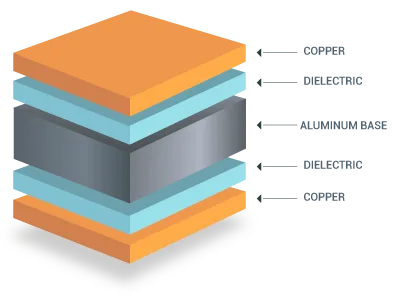
A frequent EQ comes from missing or unclear dielectric material definitions between the aluminum core and copper layers. Without specifying thermal conductivity and resin system, bonding reliability becomes uncertain during lamination.
This may lead to delamination or thermal failure under cycling conditions if not clarified early in the DFM stage.
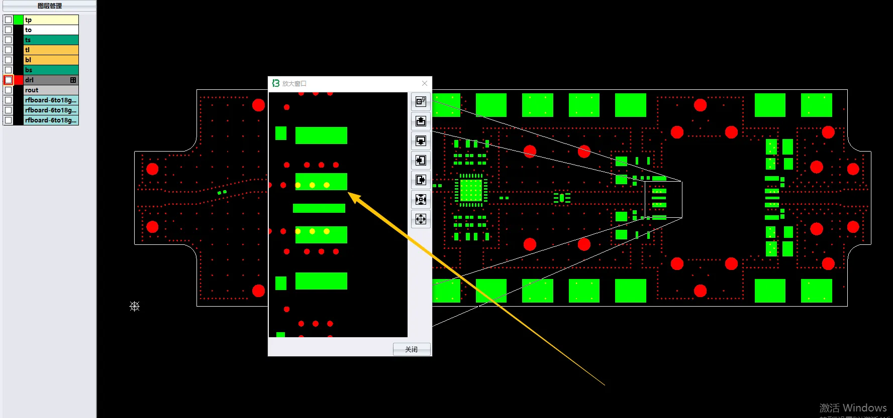
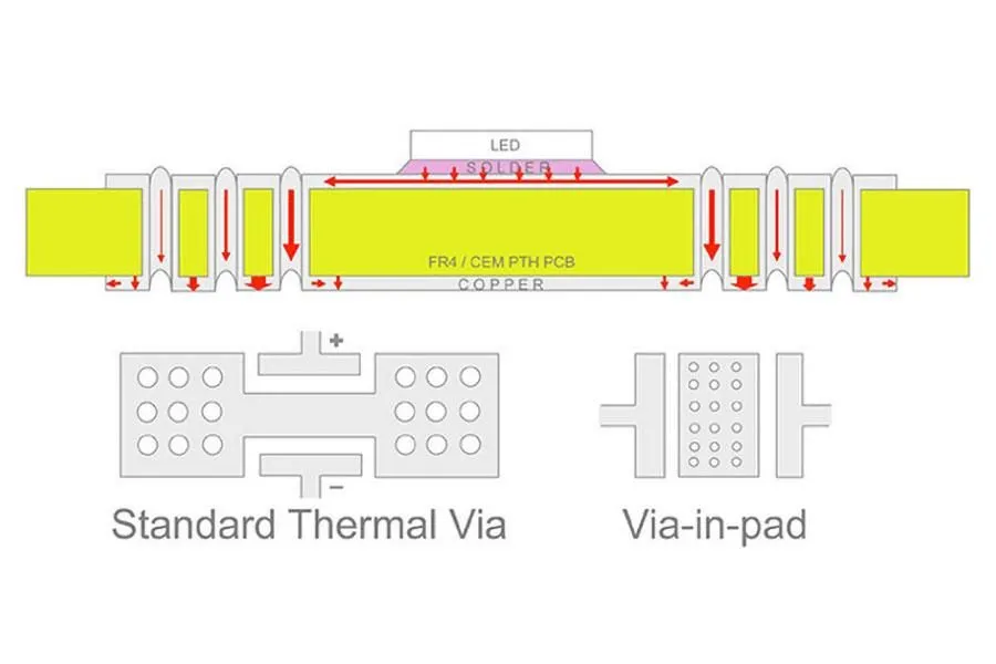
Thermal Via Design and Plating Definition
Thermal via-related EQs often occur when plating type, filling method, or aspect ratio limits are not clearly defined. Aluminum PCB processes require strict control of via structures for thermal performance.
Unclear definitions may result in voids, poor heat transfer, or plating defects affecting long-term reliability.
Solder Mask Registration and Clearance
Solder mask EQs are commonly triggered by insufficient expansion settings or misalignment risks caused by aluminum dimensional variation during processing.
If not corrected, this can lead to solder bridging, exposed copper, or reduced corrosion protection.
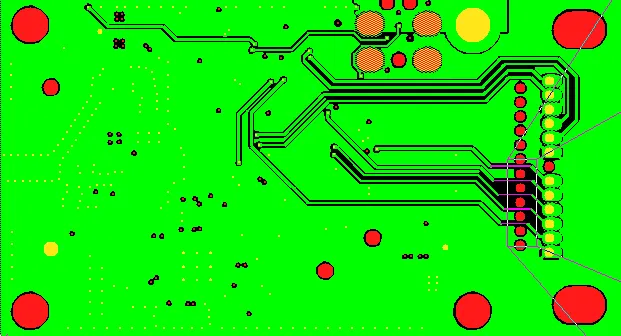
Copper Balance and Panelization Concerns
Uneven copper distribution across layers can create stress imbalance in aluminum boards, leading to warpage during lamination or reflow.
CAM systems detect these issues by analyzing copper area distribution and flagging potential mechanical instability.
Bridging the Gap: Why Standard DFM Rules Fail on Aluminum Substrates
EQs are mainly triggered because aluminum PCB manufacturing combines metal core behavior with conventional PCB processes. Standard FR4 design rules do not fully cover thermal and mechanical interactions in metal core structures.
CAM engineers must validate stack-up, via structure, and lamination compatibility to prevent defects that only appear during high-temperature or mechanical stress conditions.
How to Minimize EQs: Essential DFM Best Practices for Aluminum PCBs
To minimize engineering queries, designers should provide a complete and explicit stack-up definition, including aluminum grade, dielectric thermal conductivity, copper thickness, and bonding system.
Clear via definitions, balanced copper distribution, and proper panelization strategy significantly improve manufacturability. Early collaboration with the fabricator is strongly recommended for aluminum-based designs.
Conclusion
Two-layer aluminum PCBs can deliver excellent thermal performance when design data is fully defined and aligned with manufacturing constraints. Most EQs originate from missing or ambiguous stack-up and process details.
A well-prepared design significantly improves yield, reduces production delays, and ensures stable performance in high thermal applications.
FAQs
Q1: What is the most common reason for EQ on 2-layer aluminum PCBs?
A1: Ambiguous dielectric specifications and unclear thermal via definitions are the most common triggers. Fabricators require precise stack-up and process parameters to ensure bonding reliability and thermal performance without defects.
Q2: How does CTE mismatch affect 2-layer aluminum PCB manufacturing?
A2: Differences in thermal expansion between aluminum and copper can cause stress, warpage, or dielectric fatigue during lamination and reflow. Proper copper balancing and controlled process parameters help reduce these effects.
Q3: Should thermal vias in aluminum PCBs be plated through to the core?
A3: It depends on thermal requirements. Plated or filled vias can improve heat transfer, but they must be clearly specified to avoid process inconsistencies during fabrication.
Q4: Why is solder mask clearance critical in 2-layer aluminum designs?
A4: Aluminum core processing can introduce dimensional variation, making standard mask settings insufficient. Proper clearance prevents solder bridging and ensures reliable surface protection.
Q5: How can designers reduce warpage risks in 2-layer aluminum PCBs?
A5: Balanced copper distribution, symmetrical layout, and complete stack-up definition are key. Following manufacturer DFM guidelines significantly reduces mechanical stress and warpage risk.
References
IPC-6012E — Qualification and Performance Specification for Rigid Printed Boards. IPC, 2017
IPC-4101C — Specification for Base Materials for Rigid and Multilayer Printed Boards. IPC, 2018
IPC-MC-324 — Metal Core Circuit Board Performance Specification