Introduction
In HDI PCB production, ENIG and OSP surface finishes behave very differently when combined with microvias, blind vias, and fine pitch pads. ENIG provides excellent planarity and corrosion resistance, making it suitable for high reliability assemblies. OSP offers a cost effective and flat copper protection layer but is more sensitive to oxidation and handling conditions. These differences often lead to engineering queries during DFM review. Common concerns include via fill quality, pad flatness, and surface finish compatibility with HDI structures.
Engineering Queries in HDI: Why Precision Matters for ENIG & OSP
Engineering queries are clarification requests raised when design data does not fully align with HDI manufacturing constraints. In ENIG HDI PCB and OSP HDI PCB, these queries often relate to via-in-pad structures, solder mask definition, and surface finish compatibility. Because HDI processes involve tight tolerances and multiple plating steps, small ambiguities can lead to defects such as poor solder wetting or uneven coating. Resolving EQ early ensures stable production and reliable assembly performance.
Common EQ Types in ENIG HDI PCB and OSP HDI PCB
Via-in-pad design is one of the most frequent sources of engineering queries in HDI PCBs. Designers may specify microvias without clearly defining whether they are filled, capped, or plated over. In ENIG HDI PCB, improper via filling can lead to surface dimpling that affects gold deposition uniformity. In OSP HDI PCB, uneven via surfaces may reduce coating consistency. CAM analysis flags these issues because they directly impact solder joint reliability. Without clarification, assembly defects such as voiding or weak BGA joints may occur.
Solder mask registration issues are another common EQ trigger in HDI designs. Fine pitch pads require extremely precise alignment between mask openings and copper features. In ENIG HDI PCB, poor alignment may expose copper edges that affect plating quality. In OSP HDI PCB, incorrect mask expansion can lead to oxidation or reduced solderability. During DFM review, even small mismatches are flagged due to high reliability requirements. Proper mask definition helps eliminate these risks.
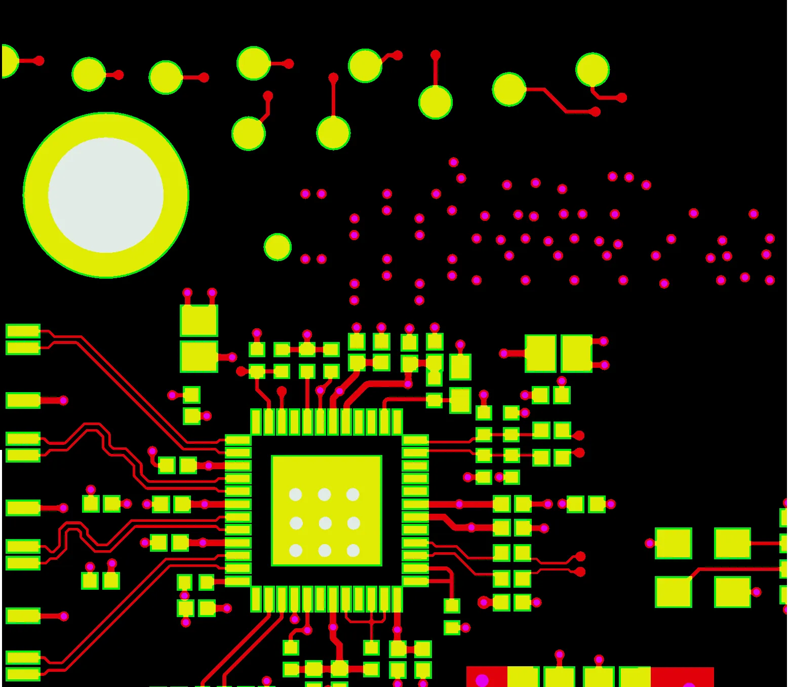
Surface finish compatibility with microvia structures also generates frequent engineering queries. ENIG HDI PCB requires highly planar surfaces to support uniform nickel and gold deposition. However, via fill shrinkage can create surface irregularities that affect plating consistency. OSP HDI PCB relies on clean copper surfaces and is sensitive to oxidation before coating. Missing process notes or unclear stackup definitions often trigger clarification requests. These issues can impact solderability and long term reliability.
Why HDI Constraints Demand Exactness
These engineering queries arise because HDI PCB manufacturing requires strict coordination between design intent and complex fabrication processes. ENIG involves multiple chemical plating steps, while OSP relies on controlled copper surface preparation. Microvia structures further increase sensitivity to process variations. During DFM review, any missing or ambiguous information is flagged to prevent downstream defects. This ensures compatibility between design data and real manufacturing capabilities.
Strategies to Eliminate EQs in High-Density Designs
To minimize EQs in ENIG HDI PCB and OSP HDI PCB, designers should clearly define via-in-pad requirements, including fill type and surface planarization. Solder mask specifications must match fine pitch HDI constraints with appropriate expansion rules. Surface finish selection should be explicitly linked to assembly conditions and component types. Providing complete stackup and fabrication notes helps eliminate ambiguity during CAM review. Early collaboration with manufacturers significantly improves first pass success rates.
Conclusion
ENIG HDI PCB and OSP HDI PCB designs require careful coordination between surface finish selection and HDI structural features such as microvias and fine pitch pads. Engineering queries commonly arise from incomplete definitions of via treatment, solder mask registration, and process compatibility. By addressing these factors early, designers can significantly improve manufacturability and reliability. Strong DFM practices ensure smoother production and higher quality HDI boards.
FAQs
Q1: What is the main difference between ENIG HDI PCB and OSP HDI PCB in manufacturing?
A1: ENIG provides a flat, corrosion resistant surface suitable for fine pitch and high reliability assemblies. OSP is a thin organic coating that protects copper but is more sensitive to handling and oxidation. Both require different DFM considerations during HDI fabrication.
Q2: Why does via-in-pad cause EQs in HDI PCB?
A2: Via-in-pad structures require precise control of filling and planarization. Without clear definitions, surface irregularities can affect soldering and plating. Manufacturers need this clarification to ensure reliability.
Q3: Is OSP suitable for HDI boards with microvias?
A3: Yes, but only when copper surfaces are properly prepared and vias are correctly processed. OSP is sensitive to surface condition, so manufacturing control is critical. Clear process documentation is required to avoid EQs.
Q4: Why does solder mask alignment matter more in HDI PCB?
A4: HDI PCBs use fine pitch pads where small misalignments can expose copper or cause bridging. Tight registration is essential for both ENIG and OSP finishes. Proper design rules reduce manufacturing risks.
Q5: How can EQs be minimized in HDI PCB design?
A5: By clearly defining via structures, surface finish requirements, and solder mask rules in fabrication notes. Providing complete stackup and assembly information helps manufacturers avoid ambiguity. Early DFM communication significantly reduces EQ volume.
References
IPC-6012E — Qualification and Performance Specification for Rigid Printed Boards. IPC, 2017
IPC-4552 — Specification for Electroless Nickel/Immersion Gold (ENIG) Plating for Printed Boards. IPC, 2017
IPC-4562 — Specification for Organic Solderability Preservative (OSP) for Printed Boards. IPC, 2013