Introduction
Multilayer HDI (High Density Interconnect) PCBs represent one of the most technically demanding product categories at AIVON. With microvias, blind and buried vias, tight tolerances, and complex stack-ups, these boards are widely used in smartphones, wearables, automotive electronics, 5G infrastructure, and high-speed computing devices where space and signal integrity are critical.
In actual engineering file reviews and CAM processing, Multilayer HDI boards generate significantly more EQs than standard multilayer FR4 due to the precision required for laser drilling, plating, registration, and impedance control. Common issues include via spacing violations, via-in-pad treatment, stack-up mismatches, and impedance line adjustments.
This article consolidates the most frequent real-world EQs observed in Multilayer HDI production, drawn directly from CAM experience and order data, and provides clear design-side prevention strategies to help engineers reduce clarification cycles and improve first-pass yield.
Case 1: Microvia Spacing and Clearance Issues
Case Overview
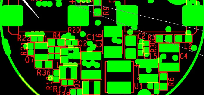
In high-density Multilayer HDI designs, microvias are frequently placed too close to each other or to adjacent traces to maximize routing density, especially in 6+ layer builds with multiple via levels.
Engineering Observation
During DFM review, CAM software flags numerous locations where via-to-via or via-to-trace spacing falls below manufacturable limits for laser-drilled microvias.
Root Cause Analysis
Designers often apply standard via rules without fully considering HDI-specific constraints such as laser drilling accuracy, plating uniformity, and registration tolerances across multiple lamination cycles.
Design Impact
Insufficient spacing leads to plating defects, short circuits, compromised impedance control, reduced yield, and potential reliability failures under thermal or mechanical stress.
Recommended Solution
The spacing between vias is too small in your design. Via-to-via spacing must be no less than 0.2mm and via-to-trace no less than 0.15mm. Please advise whether we should revise the file to maintain safe spacing.
Engineering Takeaway
In Multilayer HDI designs, always maintain via-to-via spacing ≥ 0.2mm and via-to-trace spacing ≥ 0.15mm to ensure reliable plating and high yield.
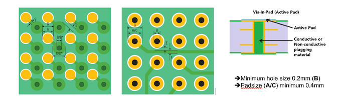
Case 2: Via-in-Pad Design and Resin Plugging Requirement
Case Overview
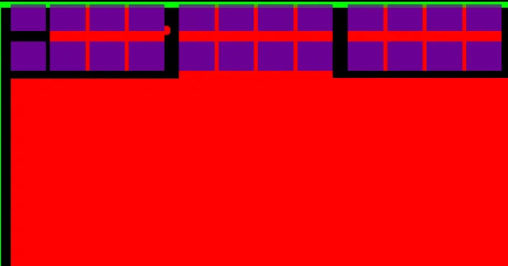
BGA or fine-pitch areas in Multilayer HDI boards commonly feature vias placed directly in pads to save space and improve signal integrity.
Engineering Observation
Engineering review identifies vias-in-pad without explicit tenting or plugging strategy specified in the files.
Root Cause Analysis
Design files often omit detailed via treatment instructions while HDI processes require explicit handling to prevent solder wicking during assembly.
Design Impact
Without proper resin plugging, risks include solder voids, shorts during reflow, and reduced long-term reliability under thermal cycling.
Recommended Solution
There are vias designed on pads. It is recommended to plug these vias with resin. Please confirm whether you accept resin plugging and any associated extra cost.
Engineering Takeaway
For vias-in-pad in Multilayer HDI designs, always specify resin plugging to ensure flat pads and reliable assembly performance.
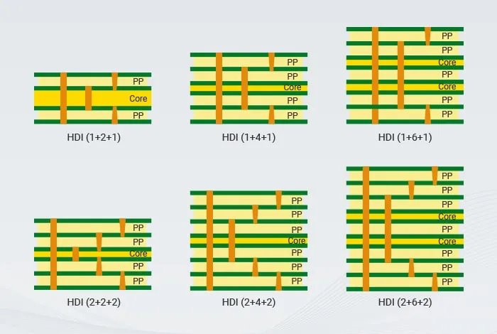
Case 3: Stack-up and Layer Sequence Confirmation
Case Overview
Customers provide initial stack-up requirements for Multilayer HDI boards that may not perfectly align with available materials and press parameters.
Engineering Observation
Layer press confirmation shows differences between requested and proposed stack-up, particularly outer layer copper thickness and dielectric materials.
Root Cause Analysis
Material inventory and HDI lamination constraints often require minor adjustments to the ideal stack-up provided in the design files.
Design Impact
Unconfirmed stack-up can cause impedance deviation, registration issues, or warpage in the final board.
Recommended Solution
Please kindly check whether the adjusted stack-up and impedance control is ok for you or not.
Engineering Takeaway
Review and approve the final factory stack-up early for all Multilayer HDI projects to avoid downstream impedance and registration problems.
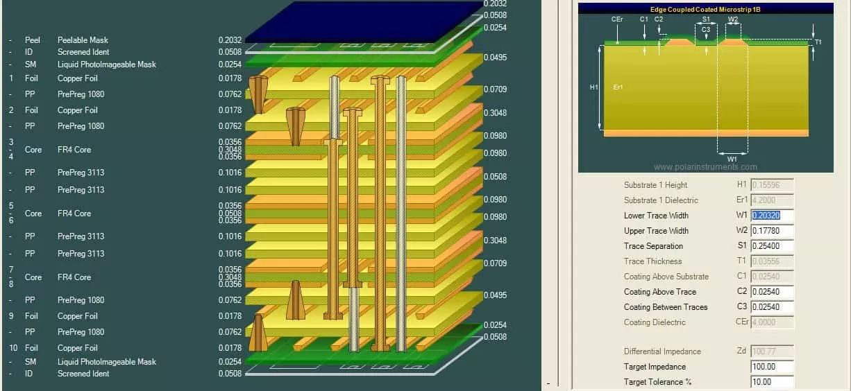
Case 4: Impedance Control Requirements and Reference Layers
Case Overview
High-speed signals in Multilayer HDI PCBs require controlled impedance lines, but files often lack clear target values or proper reference layers.
Engineering Observation
DFM check reveals impedance lines without dedicated reference planes or shielding layers.
Root Cause Analysis
Designers sometimes assume automatic impedance control without providing target values or ensuring continuous reference layers across the HDI structure.
Design Impact
Uncontrolled or deviated impedance leads to signal integrity problems, board respins, and project delays.
Recommended Solution
Please advise whether we should do impedance control for the highlighted lines and provide target values (typical single-ended 50ohm, differential 90/100ohm). Adjustments to trace width/spacing may be needed.
Engineering Takeaway
Always specify impedance targets and ensure dedicated, continuous reference layers for critical traces in Multilayer HDI designs.
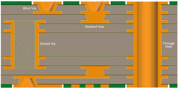
Case 5: Hole Attribute Confirmation in Complex HDI Structures
Case Overview
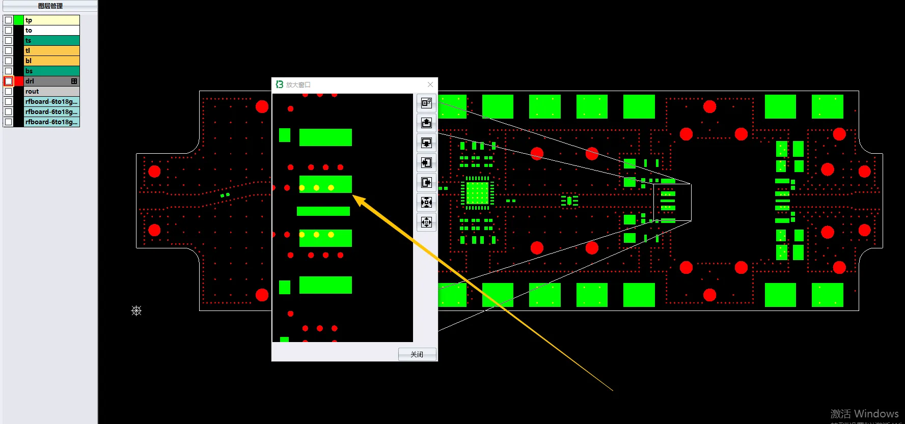
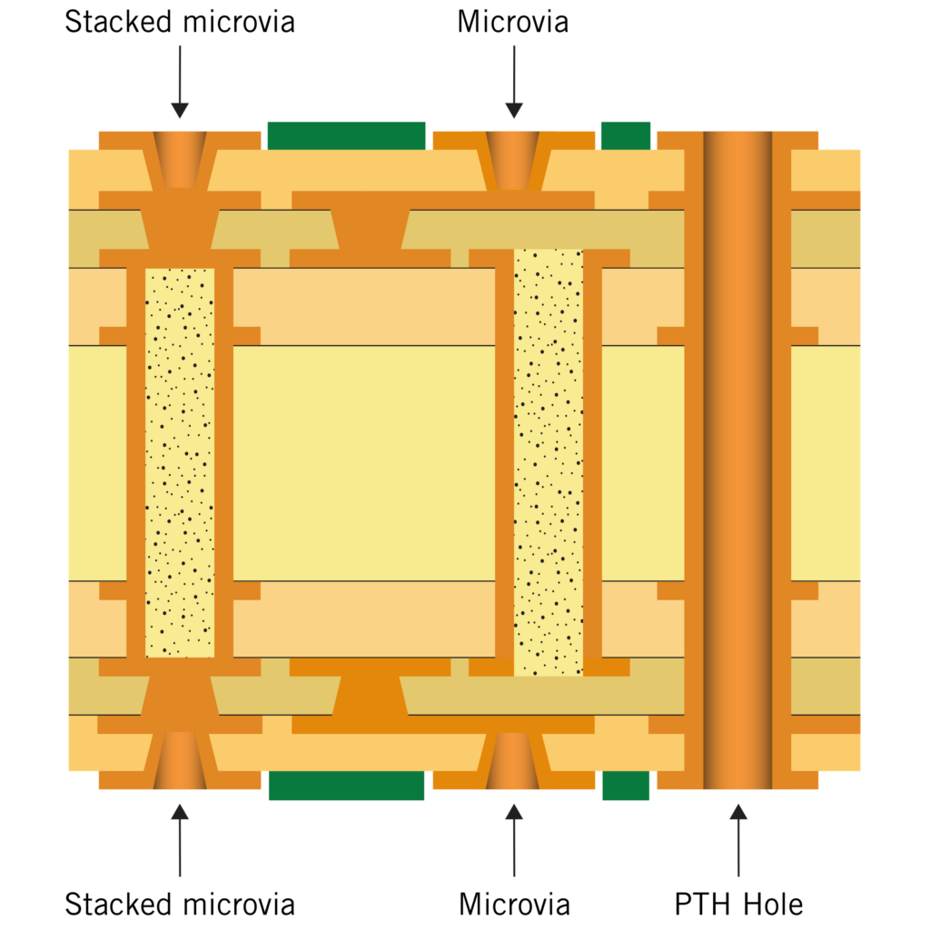
Multilayer HDI designs contain multiple via types (blind, buried, through) creating ambiguity in plating requirements.
Engineering Observation
Drill drawings and Gerber files show conflicting or unclear hole attributes at critical locations.
Root Cause Analysis
Complex HDI structures make it easy for design tools to produce unclear plating specifications between different via levels.
Design Impact
Incorrect plating decisions cause shorts, opens, or assembly problems that are difficult to debug in dense HDI boards.
Recommended Solution
Please advise whether the indicated holes should be Plated through holes or Non-plated through holes.
Engineering Takeaway
Clearly specify plating requirements (PTH/NPTH) for every hole type in Multilayer HDI Gerber files and drill drawings.
Practical Best Practices to Minimize EQ in Multilayer HDI Design
1. Provide a complete and clearly labeled stack-up drawing with target impedance values. 2. Maintain strict via spacing rules suitable for laser drilling. 3. Specify via-in-pad treatment (resin plugging) early. 4. Ensure continuous reference layers for all impedance-controlled traces. 5. Clearly define plating attributes for all via types. 6. Upload files early for a free DFM review. 7. Refer to our Multilayer HDI Manufacturing Insights before finalizing complex designs.
Conclusion
Multilayer HDI PCBs offer outstanding density and performance but require meticulous attention to via structures, stack-up, and impedance during design. By addressing the common EQs outlined above, engineers can achieve smoother production, higher yields, and faster time-to-market. For real production examples of stable HDI delivery, visit our Production Records. Ready to start your Multilayer HDI project? Get a Quote today or upload your files for a detailed engineering review.
FAQs
Q1: What is the minimum via spacing for Multilayer HDI?
A1: Via-to-via ≥ 0.2mm and via-to-trace ≥ 0.15mm is recommended to ensure reliable plating.
Q2: Should vias-in-pad be resin plugged in HDI designs?
A2: Yes, resin plugging is strongly recommended for BGA areas to prevent solder wicking and ensure flatness.
Q3: How early should stack-up be confirmed for HDI boards?
A3: As early as possible. Factory adjustments are often needed due to material availability.
Q4: Why is impedance control more challenging in HDI?
A4: Due to thinner dielectrics and multiple lamination cycles. Clear target values and reference layers are essential.
References
IPC-6012E — Qualification and Performance Specification for Rigid Printed Boards.
IPC-6013E — Qualification and Performance Specification for Flexible Printed Boards.