










PCB Silkscreen Issues: Put Orders on Hold Even After DRC Passes
Key Moment
- 0:00 Why the PCB Was Put on Hold
- 0:30 Case 1: Silkscreen Too Close to or Overlapping Pads
- 1:21 Case 2: Undersized or Overly Thin Characters
- 2:06 Case 3: Unclear or Conflicting Silkscreen Info
- 3:04 Case 4: Silkscreen & Surface Features / BGA Issues
- 4:09 How to Avoid These Problems
- 4:56 Summary & More DFM Cases Coming
What This Video Covers
This video examines four real production holds caused by silkscreen problems that passed electrical DRC checks but failed manufacturing readiness. Designers often treat silkscreen as simple geometry on screen; in fabrication it becomes physical ink subject to registration tolerances, print resolution, surface topography, and solderability constraints.
The cases cover silkscreen encroachment onto exposed pads that blocks solder wetting, characters falling below printability limits (height and stroke width), overlapping or undefined markings across Gerber layers that create intent ambiguity, and markings that interact with dense copper or BGA areas to affect ink transfer and component seating.
These issues appear across standard FR4 PCB builds, denser layouts, and boards destined for PCB assembly. The discussion shows why a clean layout review is not enough and how early DFM checks on clearance, text size, layer cleanliness, and surface interaction prevent costly holds. Engineers and procurement teams can apply the same practical limits before releasing files for a PCB prototype or volume run, then request an instant review through an online PCB quote.
Key Highlights
- Silkscreen ink on or near exposed pads is non-solderable and can create incomplete wetting or open joints during SMT; maintain practical clearance (example ~0.15 mm) and clip overlapping characters.
- Characters below typical print limits (height ≥ 0.75 mm, stroke ≥ 0.1 mm on standard processes) risk broken strokes, lost internal detail, and unreadable markings after curing.
- Clean, single-intent silkscreen layers with clearly defined locations for required markings (including production tracking) eliminate the most common engineering clarification delays.
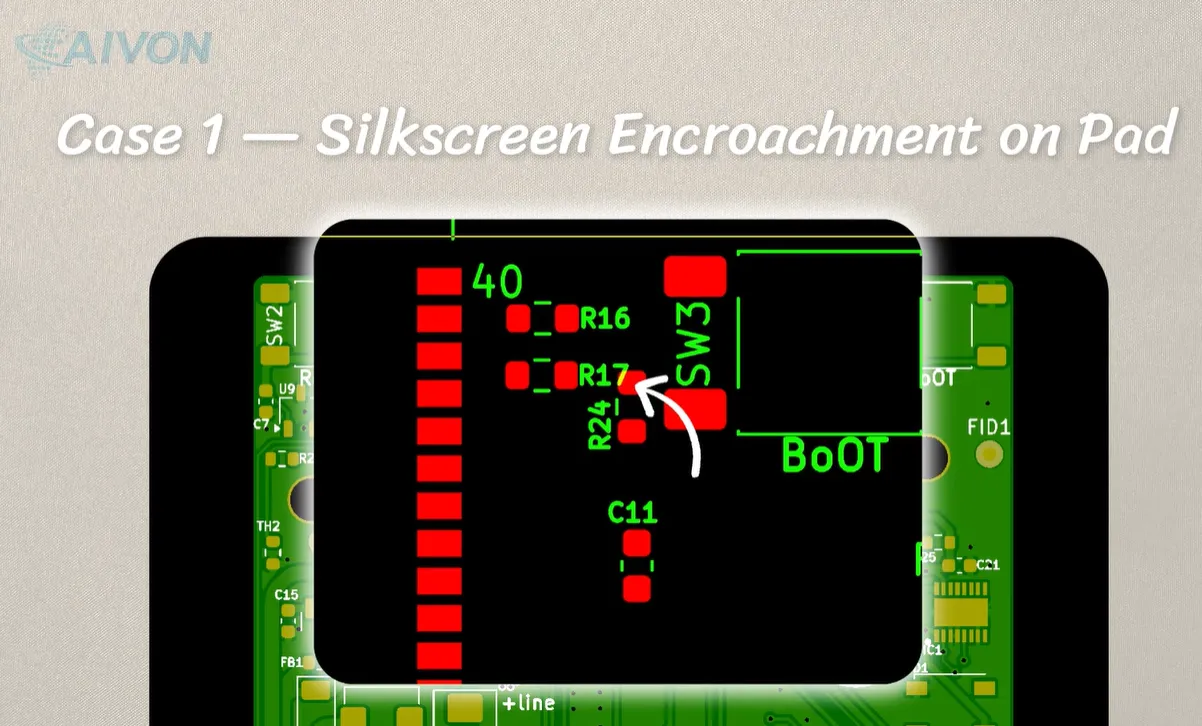
Case 1 — Silkscreen Encroachment on SMT Pads
In production, the first hold type is text or graphics that approach or enter the exposed pad area. On the CAD screen the geometry looks acceptable; once printed, the ink occupies real physical space. Because silkscreen is not solderable, any coverage of the pad surface reduces the available wetting area for solder paste.
Registration and printing tolerances mean the final ink position can shift relative to the copper. When the designed clearance is already marginal, the result is partial pad coverage. During reflow this can produce incomplete fillets, tombstoning risk on small components, or open joints that only appear in electrical test or field use.
Factory practice is to flag any encroachment and either clip the character or require a design revision. The practical engineering rule is to keep silkscreen outside the solderable region by a process-dependent margin—commonly cited around 0.15 mm for many standard processes—so that normal process variation still leaves a clean pad.
Case 2 — Undersized & Thin Characters
Dense board areas often receive small reference designators or polarity marks that appear sharp in the layout viewer. Physical screen printing, however, is limited by mesh resolution, ink rheology, and curing shrinkage. When character height or stroke width drops below the process window, strokes break, closed counters fill in, and legibility after solder-mask cure becomes unreliable.
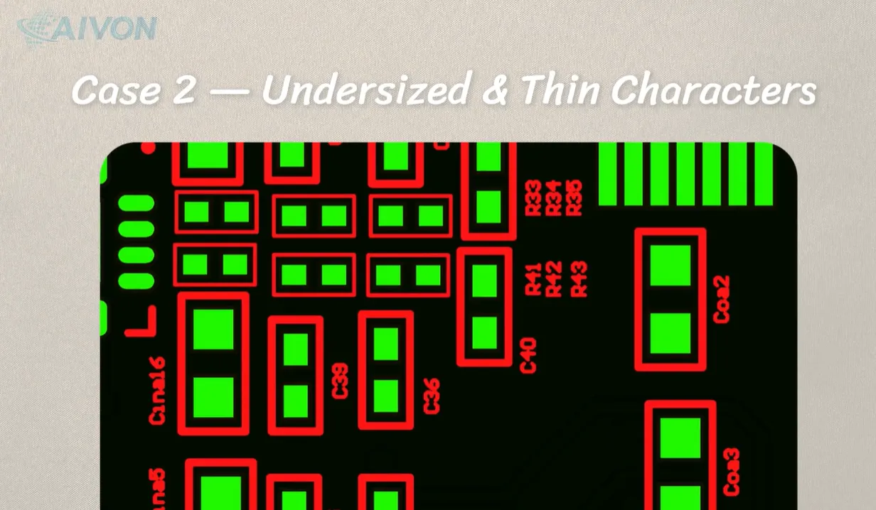
Aivon's standard silkscreen capability keeps text height at 0.75 mm or greater and stroke width at 0.1 mm or greater for consistent printability. Designs that push below these values are routinely held for confirmation or modification. The same limits apply whether the board is a simple single-sided FR4 or a more complex multilayer construction; the physics of ink transfer does not change.
Designers working in tight real-estate zones should enlarge critical markings or relocate them rather than rely on the CAD display alone.
Recommended Minimum Silkscreen Dimensions
| Parameter | Typical Minimum (Standard Process) | Risk if Violated |
|---|---|---|
| Character height | 0.75 mm | Lost detail, unreadable text |
| Stroke / line width | 0.1 mm | Broken strokes, filled counters |
| Clearance to pad | ~0.15 mm (process dependent) | Pad contamination, wetting failure |
| Clearance to other features | Process-specific | Merged ink, registration issues |
Case 3 — Unclear & Conflicting Design Information
Not every hold is geometric. Orders frequently arrive with the same text repeated across multiple Gerber layers, or with required production tracking numbers present but without a defined location or format. When layers conflict or intent is ambiguous, the engineering team must stop and confirm which data represents the true design intent.
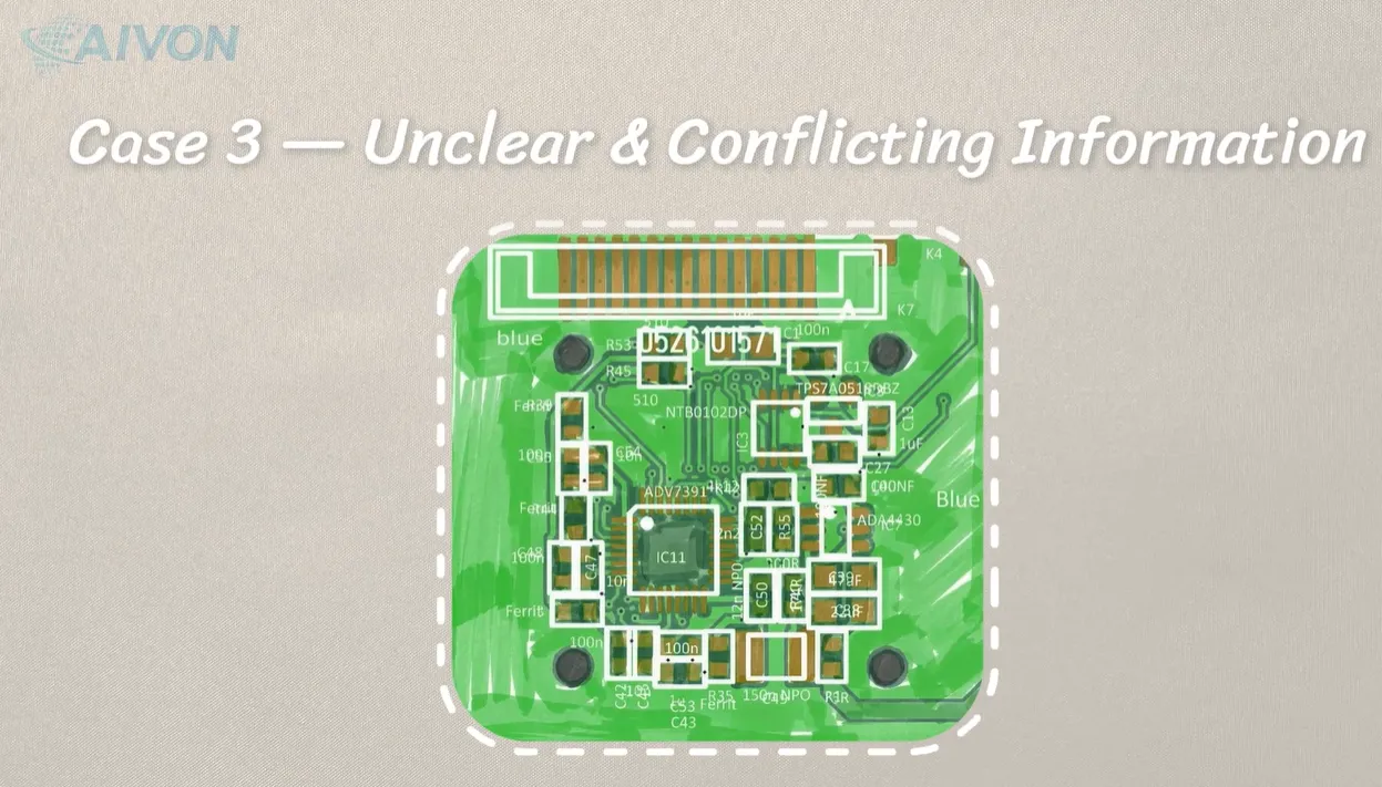
Intentional multi-layer effects are acceptable when clearly documented; undocumented overlaps are treated as potential file errors. Clean single-purpose silkscreen layers and explicit placement notes for any mandatory markings eliminate the majority of these clarification loops and keep the order on schedule.
Case 4 — Surface & Assembly Interaction Risks
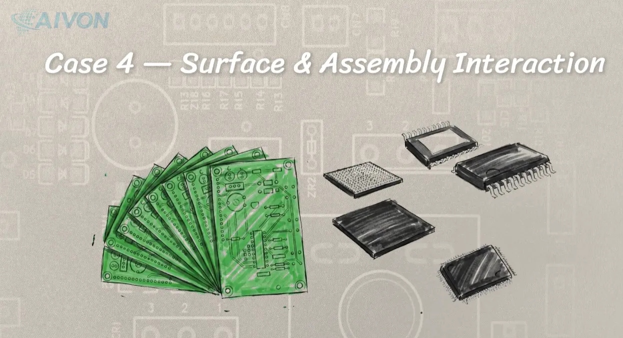
Silkscreen performance is also influenced by what lies beneath it. Dense copper patterns or solder-mask topography create local surface height differences. Ink printed across these transitions can transfer unevenly, producing broken or blurred characters.
Around BGA packages a continuous square silkscreen outline can leave a localized ink ridge. Depending on stencil design and component coplanarity, that ridge may interfere with proper seating or affect nearby solder joints. Production experience favors four discrete corner marks instead of a full box; the visual reference remains clear while the ink volume under and around the package is minimized.
These interactions are invisible in a pure electrical DRC and only become apparent when the design is reviewed against actual fabrication and assembly process capabilities.
Why Layout DRC Misses Real Manufacturing Limits
A DRC engine checks the design against the rules the designer loaded. It does not model ink spread, screen resolution, surface topography after lamination and solder-mask cure, or the mechanical seating of components during SMT. The gap between "electrically correct" and "manufacturable" is exactly where these silkscreen holds appear.
A thorough DFM review bridges that gap by applying process-specific limits rather than generic CAD rules.
Practical Pre-Production Silkscreen DFM Checks
- Verify clearance from all solderable surfaces (pads, vias, exposed copper).
- Confirm character height and stroke width meet the manufacturer's published printability window.
- Avoid continuous silkscreen across dense copper or high-topography zones.
- Keep silkscreen layers free of duplicated or undefined markings; declare any required tracking numbers with location and format.
- Review the specific DFM guidelines of the chosen fabricator—capabilities differ between processes and factories.
Early application of these checks, or submission of the files for an engineering review, removes the majority of silkscreen-related production holds.
Silkscreen Clearance & Printability Guidelines by Process
| Design Element | Standard FR4 / Multilayer | HDI / Fine-Pitch Recommendation | Notes |
|---|---|---|---|
| Pad clearance | ≥ 0.15 mm | Often tighter process window | Protects solderability |
| Min. text height | 0.75 mm | May require larger or relocated text | Print resolution limited |
| Continuous outlines near BGA | Avoid | Prefer corner marks only | Reduces ink buildup |
| Multi-layer text | Single clean layer preferred | Same | Eliminates intent ambiguity |
FAQ
Q1: What minimum silkscreen-to-pad clearance do most manufacturers require to avoid production holds?
A1: Most standard processes expect approximately 0.15 mm clearance as a practical working value; tighter designs are evaluated case-by-case against the specific print and registration capability of the factory. Encroachment is routinely flagged because silkscreen ink is non-solderable.
Q2: Can silkscreen ink on an exposed pad cause solder-joint defects in SMT assembly?
A2: Yes. Ink covering any portion of the pad reduces the solderable area, which can produce incomplete wetting, weak fillets, or open joints that only appear after reflow or during reliability testing.
Q3: Why does a board that passes DRC still get held for silkscreen issues?
A3: DRC verifies the rules loaded in the CAD system. It does not simulate physical ink transfer, surface topography after solder-mask cure, or component seating during assembly. Silkscreen problems are process and physics issues that appear only in manufacturing review.
Q4: What are typical minimum character height and stroke width for reliable PCB silkscreen?
A4: For many standard processes, character height of 0.75 mm or greater and stroke width of 0.1 mm or greater maintain printability and legibility after curing. Designs below these values risk broken strokes and unreadable markings.
Q5: How should silkscreen be designed around BGA packages to avoid assembly interference?
A5: A continuous square outline can create localized ink buildup that affects seating or nearby joints. Four discrete corner marks provide identification while minimizing ink volume in the critical area.
Why was this PCB order put on hold even though the DRC passed?
The problem wasn't a short circuit.Could it have been the silkscreen?
On screen, a silkscreen line is just geometry. In manufacturing, it becomes real ink that has to fit into real physical space — with limits on clearance, registration, and print resolution.
In this video, we'll break down real silkscreen issues found during manufacturing, and the simple design checks that can help you avoid them.
Case 1 — Silkscreen Encroachment on Pad
Here's our first real production case.
The designer placed component labels close to an SMT pad. On screen, the layout looked fine. During engineering review, our team found that the clearance between the text and the pad was very limited.In another, the ink actually extended into the exposed pad area.
Why does this matter?
Silkscreen ink is not solderable. If it covers part of an exposed pad, it can interfere with solder paste wetting during assembly, potentially leading to poor or open solder joints.
That's why silkscreen needs sufficient clearance from solderable areas. The exact limit depends on the manufacturing process, but as a practical example, a clearance of around 0.15 mm may be required.
When the clearance is too tight, the overlapping part of the character may need to be clipped or cleared to protect the solderable area.
The key takeaway is simple: what looks like harmless text on the layout still has to fit within the physical limits of the manufacturing process.
Case 2 — Undersized & Thin Characters
The second case is about character size and line width.
The designer placed small reference markings in a dense area of the board. On screen, the characters were still visible and appeared well defined.
But some of the markings were already close to the limits of the printing process, with character height and line width falling below our typical design range.
Why does this matter?
A screen can display very fine geometry with no problem. Physical silkscreen printing is different. As features become smaller, ink spread, screen resolution, and printing tolerances become more significant.
Very thin strokes can break up, while small characters can lose their internal details and become difficult to read after printing and curing.
For Aivon's standard silkscreen process, text height is generally kept at 0.75 mm or above, with text width at 0.1 mm or above to maintain printability.
Case 3 — Unclear & Conflicting Design Information
The third case was different. The challenge wasn't physical clearance or printing resolution — it was design information.
The order contained overlapping text across multiple Gerber layers, along with several markings that did not appear to serve a clear manufacturing purpose.
There was another detail as well: Some order required a production tracking number, but no specific location or format was defined in the design files.
When the same marking appears in multiple layers, or required information has no clearly defined location, the manufacturing team needs to confirm which information represents the actual design intent before moving forward.
In most cases, our engineering team will flag the conflicting layers and contact the customer to confirm what they actually want to print. But if those extra layers are intentional and that's the effect you're going for, that's totally fine. We just want to make sure it's a design choice, not a file mistake.
The takeaway here is different: not every silkscreen issue is about size or spacing. Sometimes, the most important thing is simply making sure the manufacturing team knows exactly what should be printed — and where.
Case 4 — Surface & Assembly Interaction
The fourth case goes beyond the silkscreen itself. Sometimes, what lies underneath the marking can affect how it prints — or even how nearby components are assembled.
In one order, silkscreen text was placed across an area with dense underlying features. Differences in copper and solder mask structures can create small changes in surface topography. When ink crosses these uneven areas, the transfer may become less consistent, resulting in broken or blurred markings.
A similar consideration applies around BGA components.
A solid, square silkscreen outline placed close to a BGA can create a localized layer of ink buildup. Depending on the design and process, this may interfere with component seating or potentially affect solder joint formation.
Based on production experience, engineers may recommend replacing a continuous outline with four corner marks around the BGA. This still provides clear visual identification while reducing the amount of silkscreen directly around the component.
These are details that can be easy to miss in a layout review. The marking may look perfectly fine on screen, but its position can interact with the physical surface — and with the assembly process happening around it.
why can these problems still happen when the layout looks perfectly fine?
Because a PCB layout shows us the design — but not everything that happens during manufacturing.
On screen, a line is just a line. A character is just a shape. Two layers can look perfectly clear when viewed separately.
But on a real board, ink has to be printed, surfaces have different features underneath, components have to be placed, and every process has its own limits.
That's where the gap appears.
A design can be electrically correct and still need adjustment before it can be manufactured reliably.
That's why a good DFM review goes beyond simply checking a rulebook. It connects the design with the actual manufacturing process behind it.
So, how can you avoid these issues before production?
A few simple checks can help:
Check silkscreen clearance around pads and other solderable areas.
Make sure text size and line width are within your manufacturer's printing capability.
When possible, avoid placing markings across dense or uneven areas of the board.
Keep silkscreen layers clean and clearly defined, including any required production or identification markings.
And one important point: manufacturing capabilities can vary between factories, so always check the DFM guidelines of the manufacturer you're working with.
If you're not sure whether a marking fits your manufacturer's process, checking their DFM guidelines early — or asking the engineering team to review it — can save a lot of back-and-forth later.
Silkscreen design has to work with the entire manufacturing process — not just look correct in the layout.
And if you're not sure whether your design is ready for production, a DFM review can help catch these details early.
These are not hypothetical examples. They come from real production orders and the engineering issues we encounter during review.
And silkscreen is just one category.
In this series, we'll explore more DFM cases — from copper balance and solder mask to annular rings and layer stackups — and show what happens when design meets actual manufacturing.
For more detailed breakdowns of individual production cases, visit the Aivon Blog, where we share the engineering issues behind real orders.
Catch the issue before production.





