 00:51
00:51
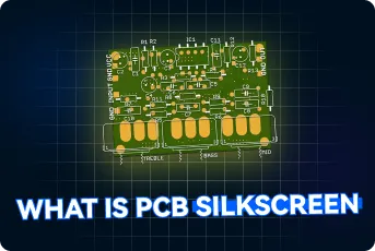
Silkscreen Design
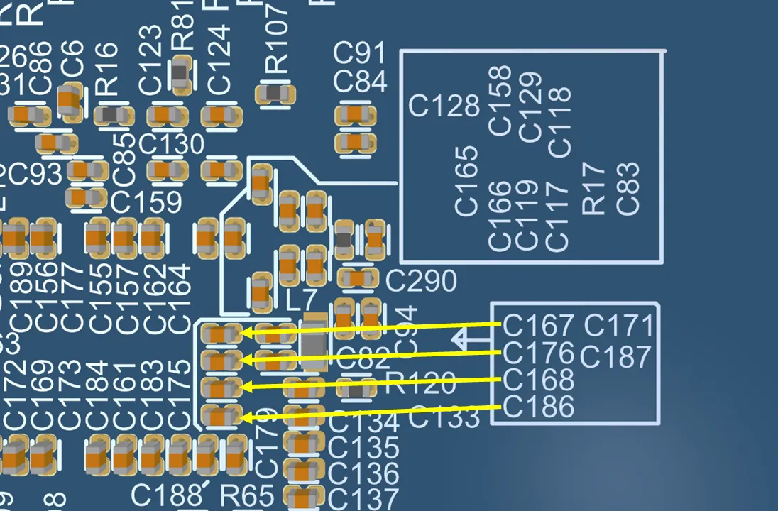
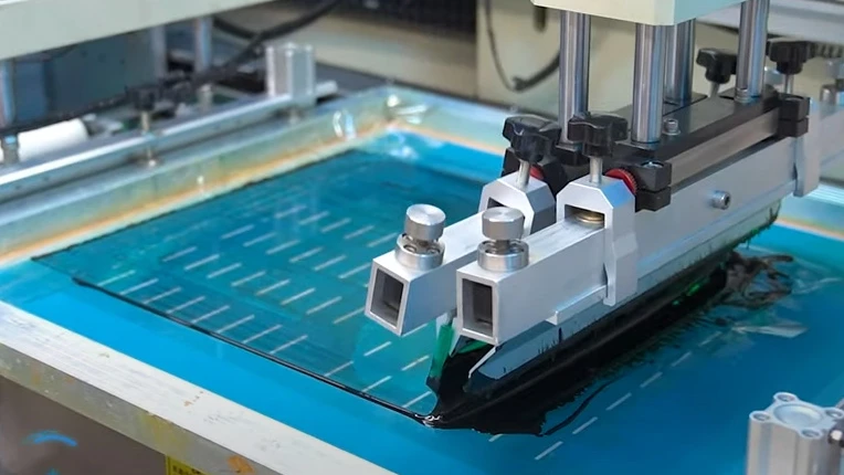
Silkscreen design plays a crucial role in printed circuit board (PCB) manufacturing, serving as the visual layer that adds text, symbols, logos, and reference markings to the board surface. This layer enhances usability by providing clear labels for components, polarity indicators, test points, and assembly instructions, which are essential for efficient production, troubleshooting, and maintenance. For engineers, hobbyists, and manufacturers searching for information on silkscreen design, this tag aggregates in-depth articles that demystify the process, from initial layout considerations to final implementation in tools like Altium Designer or KiCad. Understanding silkscreen design best practices can significantly improve PCB reliability and reduce errors during assembly. Key aspects include optimizing text size and font for readability under magnification, ensuring proper clearance from solder pads to avoid bridging issues, and selecting ink colors that contrast well with the board substrate. Articles under this tag offer actionable insights, such as guidelines for incorporating fiducials and alignment marks to streamline automated assembly lines, or tips for designing multi-layer boards where silkscreen must align precisely with underlying traces. By following these practices, designers can minimize rework and enhance the overall professionalism of their prototypes or production runs. For those tackling specific challenges, like integrating silkscreen into high-density designs or complying with industry standards such as IPC-7351, the resources here provide practical examples and case studies. Whether you are refining a new PCB layout or troubleshooting silkscreen defects in fabrication, browsing the related articles can offer targeted solutions and inspire innovative approaches to make your electronics projects more intuitive and robust.
Video Guide
-
00:51
Technical Articles
Get in Touch
Send Message
- Products & Service
- Company
- About AIVON
- Contact
- News
- Blog
- Certification
-


- Payment
-


2026 AIVON.COM All Rights Reserved