Why Silkscreen Still Matters
What This Video Covers
PCB silkscreen is often misunderstood as purely decorative text added at the end of the design process. This video reveals its true importance as a functional manufacturing and assembly layer that directly impacts production quality and efficiency.
The content explores how silkscreen defines critical elements such as component reference designators, polarity indicators, and assembly guidance markings. It details the risks when silkscreen overlaps pads, vias, or solder mask openings — elements that can be automatically clipped, shifted, or removed during PCB fabrication, potentially causing confusion on the assembly floor.
Key manufacturing considerations covered include clearance rules, minimum line width, font size, board density, and process tolerances that determine printability and legibility. Proper silkscreen design reduces rework risk, speeds up inspection, and supports accurate SMT assembly.
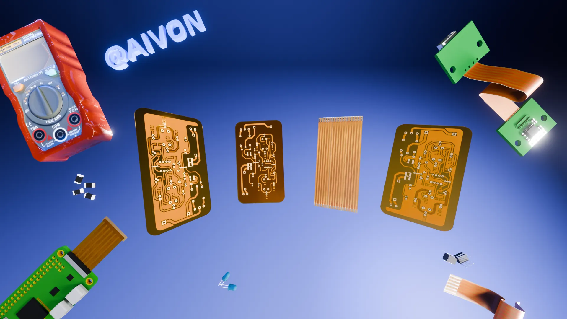
These principles apply across rigid PCB, Flexible PCB, and high-density designs used in demanding sectors. Whether prototyping or moving to volume production, treating silkscreen as a deliberate engineering decision — rather than an afterthought — improves overall reliability and manufacturing yield.
Key Highlights
Functional Role: Silkscreen provides essential reference designators, polarity indicators, and assembly guidance that directly support accurate component placement and inspection.
Manufacturing Constraints: Overlaps with pads, vias, or solder mask can cause clipping or removal; clearance rules, line width, and font size must be respected for reliable printability.
Assembly Impact: Well-designed silkscreen reduces errors, speeds up production processes, and lowers rework risk in SMT assembly.
FAQ
Q1: How does poor silkscreen design affect PCB assembly?
A1: Poor silkscreen that overlaps pads or vias can be clipped or removed during fabrication, leading to missing reference designators, polarity confusion, slower manual inspection, and higher risk of assembly errors or rework.
Q2: What are the key design rules for PCB silkscreen?
A2: Silkscreen must maintain proper clearance from pads, vias, and solder mask openings. Minimum line width, font size, and spacing should follow manufacturer tolerances to ensure legibility and prevent automatic adjustments during production.
Q3: Is silkscreen necessary for all PCB projects?
A3: While minimal or no silkscreen is possible for very simple high-volume boards, most engineering and prototyping projects benefit from clear silkscreen to support accurate assembly, testing, and long-term maintenance.
Why does silkscreen matter if the circuit already works?
Many people assume silkscreen is just text added for readability, adjusted at the end without real impact.
In fact, silkscreen is a functional layer governed by manufacturing rules.
Silkscreen defines reference designators, polarity indicators, and assembly guidance.
When it overlaps pads, vias, or solder mask openings, it can be clipped, shifted, or removed during fabrication—creating confusion on the assembly line.
Printability depends on clearance rules, line width, font size, board density, and process tolerance.
Small layout choices can affect inspection speed, assembly accuracy, and rework risk.
That's why silkscreen should be designed with manufacturing and assembly in mind.
This is aivon, making PCB learning easier, comment below — and follow for more PCB tips!