


The PCB Manufacturing Process in Action at AIVON Factory
Key Moment
What This Video Covers
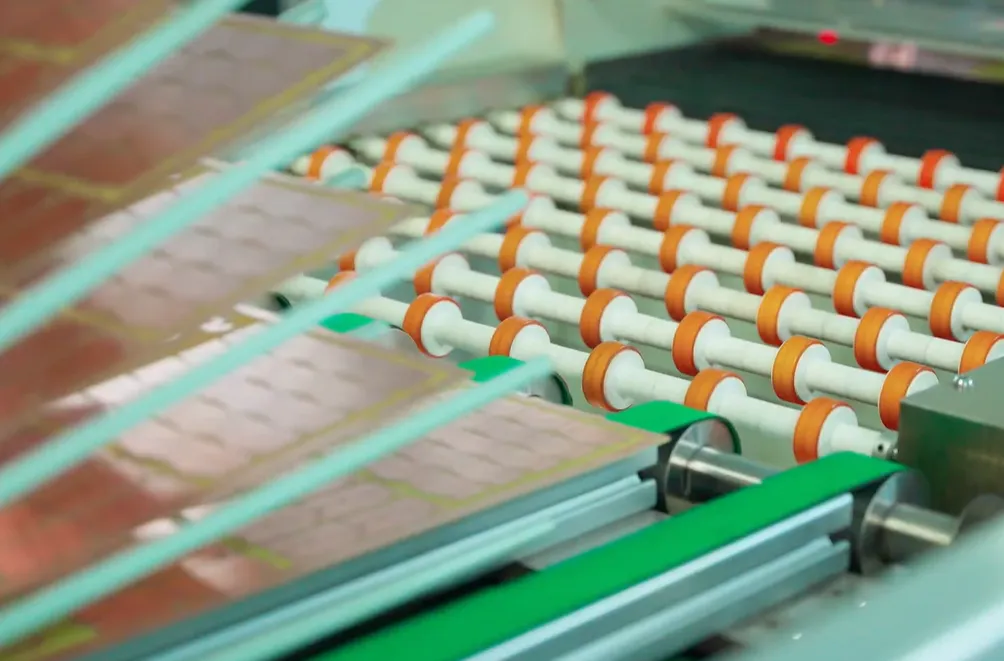
This video offers a dynamic, behind-the-scenes view of the complete PCB manufacturing process at AIVON, showing how raw materials are transformed into complex, high-reliability circuit boards. It captures the real-time flow of a fully integrated production line optimized for both speed and precision.
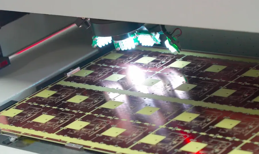
Viewers witness key stages including automated CNC drilling, sophisticated plating chemistry, lamination, etching, and high-speed optical inspection systems working in perfect synchronization. The video highlights the pristine, climate-controlled environment and advanced robotics that maintain exceptional consistency across every layer.
This manufacturing capability supports critical applications in medical devices, automotive electronics, aerospace, industrial control systems, and IoT devices, where reliability, signal integrity, and thermal management are essential. The content demonstrates AIVON's ability to deliver scalable production while maintaining tight process control.
Request an instant PCB quote to start your project. For advanced designs, explore our HDI PCB capabilities or full turnkey PCB assembly services.
Key Highlights
- Synchronized Production Line: Fully integrated automation from precision drilling to plating ensures maximum throughput and process consistency.
- Climate-Controlled Precision: Advanced robotics and optical systems operate in pristine conditions to deliver high-reliability multilayer and complex PCBs.
- End-to-End Manufacturing Excellence: Transforms engineering designs into functional boards with industrial-scale efficiency and uncompromising quality.
Critical Process Stages From Drilling Through Final Inspection
Automated CNC drilling establishes the foundation for via formation and registration accuracy. Drill bit selection, spindle speed, and feed rates must match the material stack-up; incorrect parameters produce smear, hole-wall roughness, or registration shift that later affect plating uniformity and impedance control.
Following drilling, the plating chemistry deposits copper into vias and onto surfaces. Bath composition, current density, and agitation directly influence throwing power and deposit thickness. Insufficient throwing power in high-aspect-ratio holes creates voids or thin plating that become reliability risks under thermal cycling.
Lamination bonds the layers under controlled heat and pressure. Residual moisture, uneven resin flow, or incorrect press cycles can generate delamination, voids, or warpage. After lamination, etching defines the final conductor geometry. Over-etching reduces trace width and raises impedance variation; under-etching leaves residual copper that causes shorts.
High-speed automated optical inspection and electrical testing close the process. These systems detect opens, shorts, and registration errors that visual inspection alone cannot reliably catch at production volumes.
Manufacturing Challenges That Affect Yield and Reliability
High-volume lines face recurring process risks. Drill smear on high-Tg or high-frequency materials can block plating chemicals and produce incomplete via fill. Uncontrolled plating current density creates uneven copper thickness that shifts impedance and increases risk of barrel cracking during thermal stress.
Lamination voids or resin starvation often originate from improper pre-bake of materials or incorrect vacuum and pressure profiles. These defects may pass initial electrical test yet fail later under humidity or temperature cycling. Registration drift between layers accumulates when tooling and temperature are not tightly managed, leading to annular-ring violations and reduced via reliability.
Etch-factor variation across a panel produces trace-width differences that degrade signal integrity on controlled-impedance designs. Without continuous monitoring of etchant concentration and conveyor speed, these variations remain undetected until final electrical test or field failure.
DFM Practices That Improve Consistency on Automated Lines
Designers improve manufacturability by specifying minimum annular rings that account for registration tolerance, choosing via aspect ratios compatible with the plating process, and providing clear stack-up documentation that includes dielectric thicknesses and copper weights.
Panelization strategies that balance copper distribution reduce warpage during lamination and etching. Adequate spacing between traces and planes, plus proper thermal-relief design, improves both etch uniformity and soldering performance.
Material selection should match the process capability of the line. High-frequency or high-reliability constructions benefit from materials with controlled resin content and low moisture absorption, reducing the risk of delamination and ensuring stable dielectric properties. Early design reviews that incorporate these constraints raise first-pass yield and reduce the need for engineering changes after fabrication has started.
| Process Stage | Key Control Parameters | Common Failure Mode | DFM Recommendation |
|---|---|---|---|
| CNC Drilling | Spindle speed, feed rate, bit condition | Smear, hole roughness, registration | Match drill parameters to material Tg and stack-up; allow adequate annular ring |
| Chemical Plating | Current density, bath chemistry, agitation | Voids, thin plating, uneven thickness | Limit aspect ratio; specify via fill requirements early |
| Multilayer Lamination | Temperature, pressure, vacuum, cycle time | Delamination, voids, warpage | Control copper balance; pre-bake materials as required |
| Precision Etching | Etchant concentration, conveyor speed | Trace-width variation, under/over etch | Provide balanced copper distribution; define etch factor tolerance |
| Optical & Electrical Test | Lighting, resolution, test coverage | Missed defects, false fails | Include test coupons and clear netlist data |
Applications Requiring High-Reliability Multilayer and HDI Boards
Medical devices demand stable impedance and low ionic contamination so that long-term reliability under sterilization and continuous operation is maintained. Automotive electronics require materials and processes that survive thermal cycling, vibration, and under-hood temperature extremes. Aerospace and industrial control systems further emphasize controlled dielectric thickness, tight registration, and robust via structures to ensure signal integrity under harsh environmental conditions.
The synchronized, climate-controlled production line shown in the video is designed to meet these requirements while supporting both prototype and volume quantities of multilayer, HDI, and high-frequency constructions.
FAQ
Q1: What are the main stages shown in AIVON's PCB manufacturing process?
A1: The video showcases automated drilling, chemical plating, lamination, etching, and high-speed optical inspection - all synchronized for speed and accuracy.
Q2: How does AIVON maintain quality during high-volume PCB production?
A2: Through climate-controlled facilities, advanced robotics, and continuous optical and electrical verification systems that ensure consistent results.
Q3: Is this manufacturing process suitable for complex HDI and multilayer PCBs?
A3: Yes. AIVON's production line is optimized for HDI, multilayer, rigid-flex, and high-frequency boards with tight tolerances and advanced materials.
Q4: What drilling-related issues most commonly reduce yield on automated lines?
A4: Drill smear, hole-wall roughness, and registration shift are frequent causes of plating defects and annular-ring violations. Matching drill parameters to the specific material stack-up and maintaining tight tooling control significantly reduce these failures.
Q5: How does copper balance on a panel affect lamination and etching results?
A5: Uneven copper distribution creates differential expansion and resin flow problems during lamination, leading to warpage or voids. During etching, unbalanced copper produces local etch-rate differences that alter final trace widths. Balanced copper and proper panelization improve both dimensional stability and impedance control.
Experience the pulse of modern innovation at AIVON. We're taking you behind the scenes to witness a seamless transformation—where raw materials evolve into complex high-performance circuitry.
Observe our fully integrated production line in motion. From the rapid-fire precision of automated drilling to the sophisticated chemistry of our plating lines, every stage is synchronized for maximum throughput. In our pristine, climate-controlled facility, advanced robotics and high-speed optical systems work tirelessly to maintain peak consistency.
At AIVON, we turn complex engineering designs into reality with unmatched industrial scale. This is the art of the assembly—this is PCB manufacturing in action.





