Introduction
Printed Circuit Boards (PCBs) form the backbone of modern electronics, enabling the functionality of devices across industries from consumer gadgets to aerospace systems. For electrical engineers, understanding the PCB manufacturing process is essential to ensure designs translate into reliable, high-quality products. This comprehensive guide walks through each stage of PCB fabrication, from initial design to final inspection, while aligning with globally recognized industry standards. Key aspects such as PCB etching, drilling, solder mask application, and surface finish selection are covered in detail. By grasping these steps, engineers can optimize designs for manufacturability and avoid common pitfalls during production. Whether you are refining a PCB stackup or troubleshooting fabrication issues, this article provides actionable insights to enhance your workflow.
Foundations of PCB Manufacturing: From Fabrication to Assembly
PCB manufacturing encompasses the series of processes involved in creating a functional printed circuit board from a design blueprint. It includes PCB fabrication, which focuses on building the bare board, and PCB assembly, which involves mounting electronic components onto the board. This process is critical because the quality of a PCB directly impacts the performance, reliability, and lifespan of electronic devices. A poorly manufactured PCB can lead to signal integrity issues, thermal failures, or mechanical defects. For electrical engineers, a deep understanding of the PCB manufacturing process ensures that designs are feasible for production and meet stringent requirements set by standards like those from IPC and ISO. Mastery of these steps also aids in cost optimization and faster time to market. For instance, adhering to these principles can reduce production errors by up to 30%, according to industry reports from IPC, highlighting the importance of precision from fabrication through assembly.
The PCB Manufacturing Process Steps
The PCB manufacturing process steps form the core of transforming a design into a functional board. Below, we detail each step sequentially, incorporating technical principles and best practices aligned with industry standards.
Step 1: Design and Data Preparation
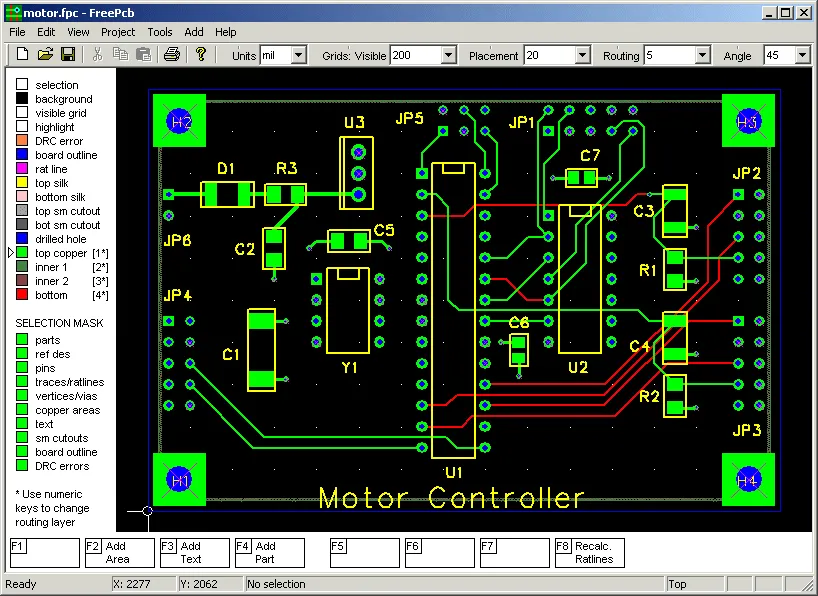
The PCB manufacturing process begins with design and data preparation, where engineers create detailed layouts using electronic design automation (EDA) tools. This stage involves defining the PCB stackup, trace widths, component placements, and generating Gerber files—standardized formats for conveying design information to manufacturers. Accurate data preparation is crucial to avoid errors in subsequent steps; for example, mismatched trace widths could lead to impedance issues in high-speed circuits. Compliance with standards such as IPC-2221B ensures designs are manufacturable and reliable, incorporating rules for minimum clearances and via sizes. Engineers often simulate signal integrity using tools like SPICE to validate designs, reducing revisions and enhancing overall efficiency.
Step 2: Inner Layer Fabrication for Multilayer Boards
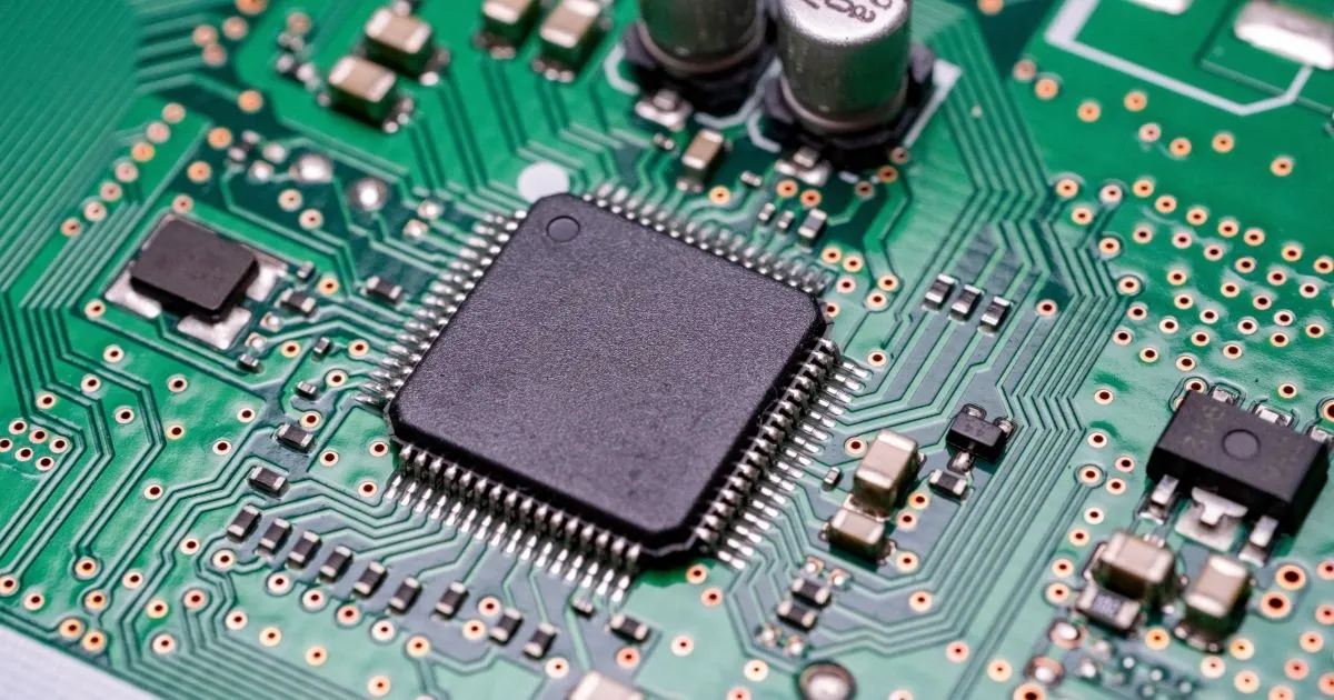
For multilayer PCBs, inner layer fabrication is a foundational step in the PCB manufacturing process. Copper-clad laminate sheets are first coated with a photosensitive film during the imaging phase, where the design pattern is transferred via ultraviolet light exposure. This is followed by etching, where unwanted copper is chemically removed to leave precise conductive traces—typically using ferric chloride or ammonium persulfate solutions for controlled material removal. After etching, the remaining photoresist is stripped away using alkaline or solvent-based strippers to reveal clean traces. Finally, Automated Optical Inspection (AOI) scans the layers for defects like shorts or opens, using high-resolution cameras and algorithms to achieve detection rates exceeding 99%. This precision is vital for maintaining trace integrity, especially in high-density interconnect (HDI) designs, and aligns with IPC-6012E standards for electrical and mechanical performance.
Step 3: Lamination and Stackup Formation
Once inner layers are prepared, lamination and stackup formation unify them into a multilayer structure. Layers are stacked with insulating prepreg material—resin-impregnated fiberglass sheets—and bonded under high heat (around 180-200°C) and pressure (up to 500 psi) in a hydraulic press. Engineers must select appropriate dielectric materials, such as FR-4 with a dielectric constant of about 4.5, and copper thicknesses (e.g., 1 oz/ft² for standard traces) to achieve desired electrical properties like controlled impedance. This step prevents delamination issues in harsh environments, such as automotive applications where thermal cycling is common. Adhering to IPC-600K acceptability criteria ensures structural integrity, with comparisons showing that optimized stackups can improve signal speed by 10-15% in multilayer boards.
Related Reading: PCB Stack Up to Plan, Design, Manufacture and Repeat
Step 4: Drilling for Vias and Through-Holes
PCB drilling creates essential holes for vias and through-hole components, marking a key transition in the PCB manufacturing process steps. High-speed CNC drills, operating at speeds up to 200,000 RPM, produce precise openings down to 0.1 mm in diameter. These holes are critical for interlayer connections and must account for material expansion to avoid cracks. For example, in a 6-layer board, blind vias might be drilled to connect only specific layers, reducing signal interference. Drilling accuracy prevents misalignment, which could cause up to 20% yield loss in production. Standards like IPC-6012E provide guidelines for hole quality, tolerances, and post-drill deburring to remove burrs that might affect plating.
Step 5: Copper Plating and Outer Layer Processing
Following drilling, copper plating reinforces the board's conductivity in the PCB manufacturing process. A thin electroless copper layer (about 1-2 microns) is first deposited chemically, followed by electrolytic plating to build up to 25-35 microns in vias and on surfaces. This ensures robust electrical connections through holes. Outer layer processing then mirrors inner layer steps: imaging transfers patterns, etching removes excess copper, and stripping cleans the board. For high-frequency applications, uniform plating thickness is crucial to minimize skin effect losses. Compliance with IPC-A-600K verifies plating quality, with techniques like cross-sectional analysis confirming adherence to specifications.
Step 6: Solder Mask Application
Solder mask application adds a protective layer to the PCB, safeguarding traces during assembly. This epoxy-based coating, often green but available in colors like blue or black, is applied via liquid photoimageable (LPI) methods or dry film, then exposed, developed, and cured at 150°C. It prevents short circuits by covering traces while exposing pads, and enhances durability against environmental factors like humidity. In high-reliability sectors like aerospace, solder mask thickness (typically 10-30 microns) must be uniform to avoid voids. IPC-SM-840E outlines performance criteria, ensuring resistance to soldering heat and chemicals.
Step 7: Silkscreen Printing
Silkscreen printing applies informative markings to the PCB surface, aiding assembly and maintenance. White or colored ink is used for component identifiers, logos, and reference designators, applied through screen-printing or inkjet methods over the solder mask. Accuracy is key; for instance, misaligned labels can complicate troubleshooting in dense SMT boards. While not affecting electrical function, clear silkscreen reduces assembly errors by 15-20%, per manufacturing studies. It complies with IPC-A-600K for visual acceptability, ensuring legibility under magnification.
Step 8: Surface Finish Selection
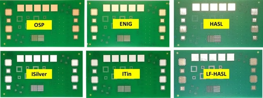
Surface finish selection protects exposed copper pads from oxidation and improves solderability in the final PCB manufacturing process steps. Options include HASL (cost-effective but lead-based variants are phased out), ENIG (offering flat surfaces and gold's corrosion resistance), and Immersion Silver (balancing cost and performance but prone to tarnish). ENIG, for example, provides a 0.05-0.2 micron gold layer over nickel, ideal for fine-pitch components. Selection depends on factors like shelf life and RoHS compliance. JEDEC J-STD-609A guides handling, with data showing ENIG reduces solder joint failures by up to 25% in humid environments.
Related Reading: Advanced Surface Finishes: Choosing the Right Option for PCB Mass Production
Step 9: Electrical Testing and Inspection
Electrical testing and inspection verify the board's integrity before assembly. Flying probe or bed-of-nails testers check for continuity, shorts, and opens, while Automated Optical Inspection (AOI) and X-ray detect hidden defects like voiding in vias. For multilayer boards, in-circuit testing might reveal issues in 5-10% of prototypes. Visual inspections ensure solder mask and silkscreen quality. Adhering to IPC-A-600K minimizes risks, with rigorous testing improving yield rates to over 95% in volume production.
Tips for Effective PCB Manufacturing
Optimizing Design for Manufacturability
To optimize the PCB manufacturing process, engineers should prioritize design for manufacturability (DFM). This includes adhering to IPC-2221B rules for minimum trace widths (e.g., 0.15 mm for standard designs) and via sizes to simplify fabrication. Simplifying the PCB stackup reduces lamination complexity, while early collaboration with fabricators prevents revisions.
Material Selection for Reliability
Material selection is key for reliability; FR-4 laminates offer a cost-thermal balance with Tg values around 130-170°C, but high-frequency applications may require Rogers materials with lower dielectric loss. Copper foil thickness (0.5-2 oz) affects current capacity—thicker foils handle higher currents but complicate etching.
Managing PCB Etching Precision
Managing PCB etching precision involves monitoring chemical baths to prevent under- or over-etching; for HDI boards, laser etching can achieve finer traces down to 50 microns. IPC-6012E guidelines ensure uniformity.
Related Reading: Advanced PCB Etching Techniques for High Density Interconnect (HDI) Boards
Streamlining PCB Assembly Processes
Streamlining PCB assembly uses SMT for efficiency, with solder paste stenciling followed by reflow at profiles per JEDEC J-STD-020E to avoid thermal damage. Automated inspection post-assembly confirms joint quality.
Troubleshooting Common Manufacturing Issues
Addressing Drilling Misalignment
Drilling misalignment can disrupt via connectivity, leading to electrical failures. This often stems from improper machine calibration or material warpage. Engineers should specify tight tolerances in design files and verify fabricator capabilities. Post-drilling inspection per IPC-6012E standards helps identify and rectify issues early.
Correcting Solder Mask Defects
Solder mask defects, such as incomplete coverage or pinholes, expose copper to oxidation. This may result from uneven application or curing issues. Adjusting exposure parameters and ensuring cleanliness during application resolves most problems. Referencing IPC-SM-840E aids in defining acceptable defect levels.
Related Reading: Solder Mask Misalignment: Causes, Consequences, and Solutions for Robust PCB Production
Preventing Surface Finish Inconsistencies
Inconsistent surface finish can hinder solderability or cause reliability issues. Variations in plating thickness or contamination are common culprits. Strict process controls and adherence to JEDEC J-STD-609A during application ensure uniform finish quality across batches.
Conclusion
The PCB manufacturing process is a complex sequence of steps that transforms design concepts into functional boards. From initial data preparation to final surface finish application, each stage demands precision and adherence to industry standards like those from IPC and JEDEC. Electrical engineers who understand PCB fabrication, etching, drilling, and assembly can better optimize designs for reliability and cost efficiency. By focusing on material selection, process control, and thorough inspection, potential issues can be minimized. This guide serves as a foundation for navigating the intricacies of PCB production, ensuring high-quality outcomes for diverse applications.
FAQs
Q1: How does PCB etching impact the quality of a printed circuit board?
A1: PCB etching directly affects trace accuracy and electrical performance. If not controlled, over-etching can thin traces, increasing resistance, while under-etching may leave unwanted copper, risking shorts. Following standards like IPC-6012E ensures precise removal of excess copper. Proper chemical monitoring and process adjustments are essential for consistent results, especially in high-density designs.
Q2: What factors should engineers consider during PCB drilling?
A2: During PCB drilling, engineers must consider hole size, placement accuracy, and material properties. Misaligned or oversized holes can disrupt connectivity in vias or through-hole components. Specifying tolerances as per IPC-6012E and selecting appropriate drill speeds prevent defects. Material warpage should also be minimized to maintain precision across the board.
Q3: Why is solder mask application critical in PCB manufacturing?
A3: Solder mask application protects copper traces from oxidation and prevents short circuits during assembly. It ensures only designated pads are exposed for soldering, enhancing reliability. Defects like pinholes can compromise this protection. Adhering to IPC-SM-840E standards during application guarantees durability and performance under various environmental conditions.
Q4: How does surface finish selection influence PCB assembly outcomes?
A4: Surface finish selection impacts solderability and long-term reliability in PCB assembly. Finishes like ENIG offer excellent corrosion resistance, while HASL is cost-effective but less uniform. Choosing the right finish per JEDEC J-STD-609A ensures compatibility with soldering processes and environmental stresses. This decision affects both assembly quality and product lifespan.
References
IPC-2221B — Generic Standard on Printed Board Design. IPC, 2012.
IPC-6012E — Qualification and Performance Specification for Rigid Printed Boards. IPC, 2020.
IPC-A-600K — Acceptability of Printed Boards. IPC, 2020.
IPC-SM-840E — Qualification and Performance of Permanent Solder Mask and Flexible Cover Materials. IPC, 2011.
IPC-4101E — Specification for Base Materials for Rigid and Multilayer Printed Boards. IPC, 2017.
JEDEC J-STD-020E — Moisture/Reflow Sensitivity Classification for Nonhermetic Surface Mount Devices. JEDEC, 2014.
JEDEC J-STD-609A — Marking and Labeling of Components, PCBs and PCBAs to Identify Lead (Pb), Lead-Free (Pb-Free) and Other Attributes. JEDEC, 2011.


