Introduction
In the realm of printed circuit board development, the stack-up serves as the foundational blueprint that dictates performance, reliability, and manufacturability. A well-planned PCB stack-up ensures optimal signal integrity, supports high-speed applications, and accommodates complex designs like high-density interconnect (HDI) and hybrid stackups. For electrical engineers, understanding how to plan, design, and manufacture these configurations is critical to meeting stringent project demands. This article explores the intricacies of PCB stack-up design with a focus on HDI, hybrid stackup, high-speed, rigid, and rigid-flex boards. It also addresses signal integrity and key manufacturing aspects to achieve consistent, repeatable results. Whether working on compact consumer electronics or robust industrial systems, mastering stack-up strategies can significantly enhance outcomes.
What Is PCB Stack-Up and Why It Matters
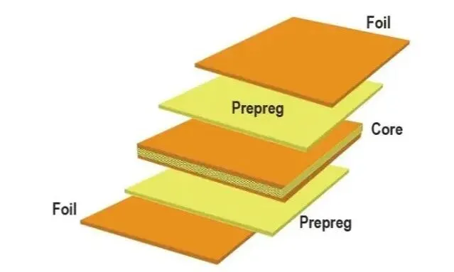
A PCB stack-up refers to the arrangement of conductive and insulating layers within a printed circuit board. It defines the number of layers, their sequence, and the materials used, directly impacting electrical performance and structural integrity. For high-speed designs, the stack-up influences impedance control and crosstalk reduction. In HDI PCBs, it enables tighter routing with microvias for compact layouts. Hybrid stackups, combining rigid and flexible sections, offer versatility for unique form factors. Signal integrity, a critical concern, depends on proper layer planning to minimize noise and ensure reliable data transmission. From a manufacturing aspect, the stack-up determines fabrication complexity, cost, and feasibility. A poorly planned stack-up can lead to delays, defects, or performance failures, making it a pivotal element in the design process for engineers.
Technical Principles of PCB Stack-Up Design
The design of a PCB stack-up is governed by several engineering principles that ensure functionality across various applications. Layer arrangement is a primary consideration. In high-speed designs, signal layers are often sandwiched between ground planes to reduce electromagnetic interference. This configuration helps maintain signal integrity by providing a consistent return path for currents. For deeper insights into high-speed applications, explore our PCB stack-up design guide for high-speed signals.
For HDI boards, the use of microvias and buried vias allows for denser routing. These small-diameter vias connect specific layers without penetrating the entire board, saving space and improving electrical performance. However, they require precise alignment during manufacturing to avoid defects. Hybrid stackups, which may include both rigid and rigid-flex sections, demand careful material selection to balance mechanical stress and flexibility.
Impedance control is another crucial factor, especially in high-speed applications. The dielectric thickness and material properties between layers must be calculated to match the required impedance values. Deviations can lead to signal reflections and data loss. Thermal management also plays a role, as power layers need adequate copper thickness to handle current without overheating.
Standards such as IPC-2221B, which provides guidelines for PCB design, emphasize the importance of layer symmetry to prevent warpage during fabrication. Following such established frameworks ensures that designs are practical and manufacturable.

Best Practices for Planning and Designing PCB Stack-Ups
Creating an effective PCB stack-up begins with a clear understanding of project requirements. Engineers should start by defining the number of layers needed based on routing density and component placement. For HDI designs, incorporating microvias early in the planning phase can optimize space. It is essential to collaborate with manufacturing teams to confirm that the chosen configuration aligns with fabrication capabilities.
In high-speed designs, prioritize placing signal layers adjacent to reference planes. This setup minimizes loop inductance and enhances signal integrity. Use simulation tools to model impedance and identify potential issues before finalizing the design. For hybrid stackups involving rigid and rigid-flex sections, ensure that transitions between materials are smooth to avoid mechanical stress points. Selecting compatible dielectric materials with similar thermal expansion properties is vital. See our detailed 8-layer PCB stackup design example.
Symmetry in layer arrangement helps mitigate manufacturing issues like bowing or twisting. Adhering to guidelines in IPC-6012E for rigid board performance ensures that designs remain stable under thermal and mechanical stress. Additionally, plan for adequate spacing between layers to prevent crosstalk, especially in high-speed applications. Documenting all design parameters thoroughly aids in maintaining consistency during production runs.

Manufacturing Aspects of PCB Stack-Ups
From a manufacturing perspective, the stack-up design directly influences production complexity and yield. HDI boards, with their intricate via structures, require advanced lamination and drilling processes. Sequential lamination, often used for such designs, builds the board in stages, adding layers progressively. This method demands precise control to ensure alignment and avoid defects.
For rigid and rigid-flex PCB hybrid stackups, manufacturing involves bonding different materials, which can introduce challenges like delamination if not handled correctly. Following standards like IPC-A-600K for acceptability criteria ensures that manufactured boards meet quality benchmarks. Signal integrity concerns also extend to production, where variations in dielectric thickness or copper etching can affect performance. Tight process controls are necessary to maintain consistency.
Engineers must provide detailed stack-up documentation to fabricators, specifying layer order, materials, and tolerances. This clarity reduces errors and facilitates repeatable results across batches. Thermal cycling during manufacturing, guided by standards like IPC-6012E, tests the board's resilience to stress, ensuring reliability in end-use applications.

Signal Integrity Considerations in Stack-Up Design
Signal integrity remains a cornerstone of effective PCB stack-up design, particularly for high-speed applications. Proper layer planning can significantly reduce issues like crosstalk, signal delay, and reflections. Positioning high-speed signal traces close to a continuous ground plane creates a controlled impedance environment, essential for maintaining data integrity.
In HDI designs, shorter signal paths enabled by microvias help minimize latency and improve performance. However, engineers must avoid via stubs, which can act as antennas and introduce noise. Back-drilling or using blind vias, as recommended in industry practices, can eliminate these stubs. For hybrid stackups, signal routing through flexible sections requires careful attention to maintain consistent impedance across transitions.
Simulation and analysis before fabrication are critical steps. Tools that model electromagnetic behavior can predict potential signal integrity issues, allowing adjustments in the stack-up design. Adhering to guidelines in IPC-2226 for HDI structures ensures that designs are optimized for performance and manufacturability.
Troubleshooting Common Stack-Up Challenges
Even with meticulous planning, stack-up designs can encounter issues during design or manufacturing phases. Warpage is a frequent problem, often caused by asymmetrical layer arrangements or mismatched material properties. Ensuring symmetry and consulting standards like IPC-6012E can prevent such defects. If warpage occurs, reviewing thermal expansion coefficients of materials used may identify the root cause.
Signal integrity failures, such as excessive crosstalk, often stem from inadequate spacing between traces or improper grounding. Revisiting the stack-up to add more ground planes or adjust layer spacing can resolve this. In HDI boards, misaligned microvias can disrupt connectivity. Close coordination with manufacturers to verify drilling precision is essential in such cases.
For rigid-flex hybrid stackups, mechanical failures at transition zones are common. Reinforcing these areas with additional adhesive layers or adjusting the design to reduce stress concentration can help. Thorough testing under simulated operating conditions ensures that the stack-up performs as intended.
Case Studies & Real-World Stackup Examples
A leading 5G base-station manufacturer used an 8-layer symmetrical HDI stack-up with two sequential lamination cycles. By placing high-speed signals on layers 2 and 7 adjacent to ground planes and using filled microvias, they achieved 28% lower insertion loss at 28 GHz and reduced crosstalk by 22 dB compared to their previous 6-layer design.
In an automotive ADAS project, engineers implemented a 6-layer hybrid rigid-flex stack-up. Careful material selection with matching CTE values eliminated warpage issues that had previously caused 15% yield loss. The final design supported 112 Gbps PAM4 signaling while surviving 1,000 thermal cycles from –40 °C to +125 °C.
Future Trends in PCB Stack-Up Design
Emerging trends include AI-assisted stack-up optimization tools that automatically generate impedance-controlled configurations based on target frequencies and power requirements. Advanced low-loss materials such as glass-core substrates and hybrid organic-ceramic laminates are enabling sub-0.5 dB/inch insertion loss at 100 GHz. Embedded component stack-ups and 3D-printed dielectric layers are expected to reduce board thickness by 30–40% while improving thermal performance. By 2028, fully automated stack-up validation integrated with manufacturing execution systems will become standard for high-volume production.
Conclusion
A well-executed PCB stack-up is the backbone of any successful circuit board project, influencing everything from signal integrity to manufacturing efficiency. By carefully planning and designing stack-ups for HDI, high-speed, rigid, and rigid-flex applications, engineers can achieve optimal performance and reliability. Attention to manufacturing aspects ensures that designs translate seamlessly from concept to production. Embracing industry standards and best practices facilitates repeatable results, reducing risks of failure. As technology advances, staying informed about evolving stack-up strategies will remain essential for tackling complex design challenges and delivering high-quality solutions.
FAQs
Q1: What factors impact signal integrity in a PCB stack-up for high-speed designs?
A1: Signal integrity in high-speed designs depends on layer arrangement, impedance control, and grounding. Placing signal layers near ground planes reduces noise and crosstalk. Proper dielectric thickness ensures consistent impedance, while avoiding via stubs prevents reflections. Following industry guidelines helps maintain reliable data transmission under demanding conditions.
Q2: How does HDI stack-up design differ from traditional PCB layouts?
A2: HDI stack-ups utilize microvias and buried vias for denser routing, unlike traditional layouts with larger through-hole vias. They support compact designs with finer traces, requiring precise manufacturing control. HDI configurations often involve sequential lamination, adding complexity compared to standard multilayer boards, but enable superior performance.
Q3: What are key manufacturing aspects to consider for rigid-flex hybrid stackups?
A3: Manufacturing rigid-flex hybrid stackups requires managing material transitions to prevent delamination. Bonding rigid and flexible layers demands precise alignment and compatible adhesives. Thermal stress during production must be controlled to avoid warpage. Clear documentation and adherence to quality standards ensure consistent results across production runs.
Q4: Why is symmetry important in a PCB stack-up for rigid boards?
A4: Symmetry in rigid PCB stack-ups prevents warpage during thermal cycles in manufacturing. Balanced layer distribution reduces mechanical stress, ensuring flatness and reliability. Asymmetrical designs can lead to bowing, impacting assembly and performance. Industry standards emphasize symmetry for structural integrity and long-term durability.
References
IPC-2221B — Generic Standard on Printed Board Design. IPC, 2012.
IPC-2226 — Sectional Design Standard for High Density Interconnect (HDI) Printed Boards. IPC, 2003.
IPC-6012E — Qualification and Performance Specification for Rigid Printed Boards. IPC, 2020.
IPC-A-600K — Acceptability of Printed Boards. IPC, 2020.