


Inside AIVON PCB Factory: Precision Manufacturing Process
Key Moment
What This Video Covers
This video takes viewers inside AIVON's state-of-the-art PCB manufacturing facility, showcasing the complete journey from raw substrate to finished circuit board. It highlights how modern PCB fabrication combines advanced automation with strict quality control to achieve both exceptional precision and impressive production speed.
The tour covers key stages of the manufacturing process, including substrate cutting, lamination, etching, drilling, plating, and final inspection. Viewers will see the ultra-clean environment and automated equipment that ensure consistent quality across rigid, flexible, and complex multilayer boards.
AIVON's facility is engineered to support demanding applications such as medical devices, automotive electronics, aerospace, and industrial control systems, where reliability and signal integrity are critical. The video demonstrates why choosing the right manufacturing partner matters for both PCB prototype and volume production needs.
Get an instant quote for your next project. For higher complexity designs, explore our HDI PCB and rigid-flex PCB capabilities. Teams requiring full turnkey solutions can also review our PCB assembly services.
Key Highlights
- Ultra-Clean Automated Production: Advanced equipment and controlled environments ensure maximum reliability across every stage of PCB fabrication.
- End-to-End Precision Process: From initial substrate handling through lamination, drilling, plating, and final inspection for consistent high-quality results.
- Speed with Quality: Modern manufacturing systems that deliver fast turnaround without compromising engineering standards.
Complete Fabrication Sequence from Substrate Cutting to Final Inspection
The video walks through each major process step in sequence. Substrate panels are first cut and prepared under controlled conditions to maintain dimensional stability. Lamination follows, where prepreg and copper foils are bonded under precise temperature, pressure, and vacuum parameters to form the multilayer stack.
Etching defines the circuit patterns with tight line-width and spacing control. Mechanical and laser drilling create vias and holes, followed by electroless and electrolytic plating that deposits copper for reliable interconnects. Surface finishing and final electrical testing complete the sequence.
Each transition between stages is monitored for registration accuracy and contamination risk. In real production, even small deviations in lamination pressure or drill registration can produce voids, delamination, or open vias. The automated flow shown in the video minimizes these risks by maintaining consistent process windows and reducing manual handling.
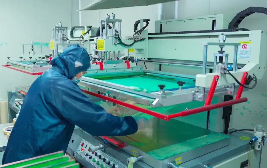
Ultra-Clean Automated Environments and Equipment in Operation
Cleanroom conditions and automation form the foundation of yield stability. The facility maintains controlled particulate levels, temperature, and humidity so that sensitive processes such as photoresist application, etching, and plating remain free of contamination.
Automated material handling systems move panels between stations with minimal human contact, reducing the chance of scratches, fingerprints, or particle introduction. Real-time monitoring of equipment parameters—drill bit wear, plating bath chemistry, and etch rates—allows immediate correction before defects accumulate.
In high-layer-count or fine-pitch designs, contamination or process drift frequently causes intermittent opens, shorts, or impedance shifts that only appear after assembly. The ultra-clean automated environment demonstrated in the video directly addresses these failure modes by keeping critical process variables within narrow tolerances from the first panel to the last.
Process Controls That Protect Signal Integrity and Yield
Signal integrity and long-term reliability depend on more than just clean equipment. Controlled copper thickness, uniform dielectric spacing, and accurate via formation are essential for high-speed and high-frequency boards.
The video illustrates how plating uniformity and drill registration are maintained across large panel sizes. Inadequate control in these areas commonly leads to barrel cracks, poor via fill, or impedance variation that fails downstream testing or field reliability requirements.
DFM best practice requires designers to align stack-up choices, via aspect ratios, and copper balance with the factory's proven process capabilities. When these parameters are matched, the risk of scrap and schedule delays drops significantly. The factory's process controls shown in the tour provide the measurable consistency needed for medical, automotive, and aerospace boards where field failures carry high consequences.
| Process Stage | Critical Parameter Controlled | Common Failure Mode Avoided | DFM Recommendation |
|---|---|---|---|
| Lamination | Temperature, pressure, vacuum | Delamination, voids | Balanced copper distribution, proper prepreg selection |
| Drilling | Registration accuracy, bit wear | Misaligned vias, broken bits | Aspect ratio ≤ 10:1 for mechanical drills |
| Plating | Bath chemistry, current density | Thin copper, voids in vias | Specify minimum copper thickness in holes |
| Final Inspection | Electrical continuity, AOI | Escaped opens/shorts | Include test coupons and impedance targets |
Scaling Reliability from Prototype to Volume Production
Prototype panels and volume production must share the same process recipe if quality is to remain consistent. The video shows equipment and cleanroom infrastructure sized to support both quick-turn prototypes and larger production runs without changing fundamental process settings.
When factories treat prototypes as special cases, subtle differences in lamination cycles or plating chemistry can produce boards that pass initial tests but fail in volume. Maintaining identical process windows eliminates this risk. Designers benefit by receiving early feedback on manufacturability that remains valid when quantities increase.
Material handling, panelization strategies, and inspection sampling plans are also scaled in a controlled manner so that yield data from prototypes accurately predict volume performance. This continuity is a practical advantage for projects that move rapidly from engineering validation to production release.
Supporting Demanding Applications in Medical, Automotive, and Aerospace
Boards for medical devices, automotive electronics, and aerospace systems require documented process control and high reliability. The facility's combination of cleanroom discipline, automated process monitoring, and end-to-end inspection supports the material and construction types commonly specified for these markets—FR4, high-Tg laminates, Rogers materials, aluminum substrates, HDI, and rigid-flex constructions.
In these applications, even low-level contamination or uncontrolled plating thickness can compromise long-term insulation resistance or thermal cycling performance. The manufacturing environment and process discipline shown in the video are structured to keep such risks under control across both prototype and production volumes.
FAQ
Q1: What makes AIVON's PCB factory different from standard manufacturers?
A1: AIVON combines an ultra-clean production environment with highly automated equipment and professional engineering oversight, enabling both rapid turnaround and superior reliability for complex boards.
Q2: Which types of PCBs can AIVON manufacture in their factory?
A2: The facility supports rigid PCBs, flexible circuits, rigid-flex, HDI, high-frequency, and multilayer boards using materials like FR4, Rogers, and aluminum.
Q3: Does AIVON support both prototype and mass production volumes?
A3: Yes. Our factory is optimized for quick-turn PCB prototyping as well as scalable mass production with consistent quality controls throughout.
Q4: How does the factory control registration accuracy during multilayer drilling?
A4: Automated optical alignment and real-time drill monitoring maintain registration within tight tolerances. This reduces the risk of misaligned vias that can cause opens or reliability issues in high-layer-count boards. Designers should still keep aspect ratios and pad sizes within the factory's published capabilities to maximize yield.
Q5: What common DFM issues are prevented by the ultra-clean automated process?
A5: Particle contamination, uneven plating, and lamination voids are minimized through controlled environments and continuous process monitoring. These defects frequently appear as intermittent failures after assembly or during thermal cycling. Matching the design's copper balance, via structures, and material selection to the factory's process window further reduces risk.
Step inside AIVON, where cutting-edge technology meets manufacturing excellence. From the initial substrate cutting to meticulous final inspection, witness a production journey defined by surgical precision.
Our state-of-the-art facility combines a pristine, ultra-clean environment with the latest automated equipment to ensure maximum reliability. At AIVON, we don't just manufacture circuit boards; we engineer the backbone of modern electronics. Every layer and every trace is a testament to our commitment to quality and efficiency.
This is the future of PCB fabrication. This is AIVON—where precision truly meets speed.





