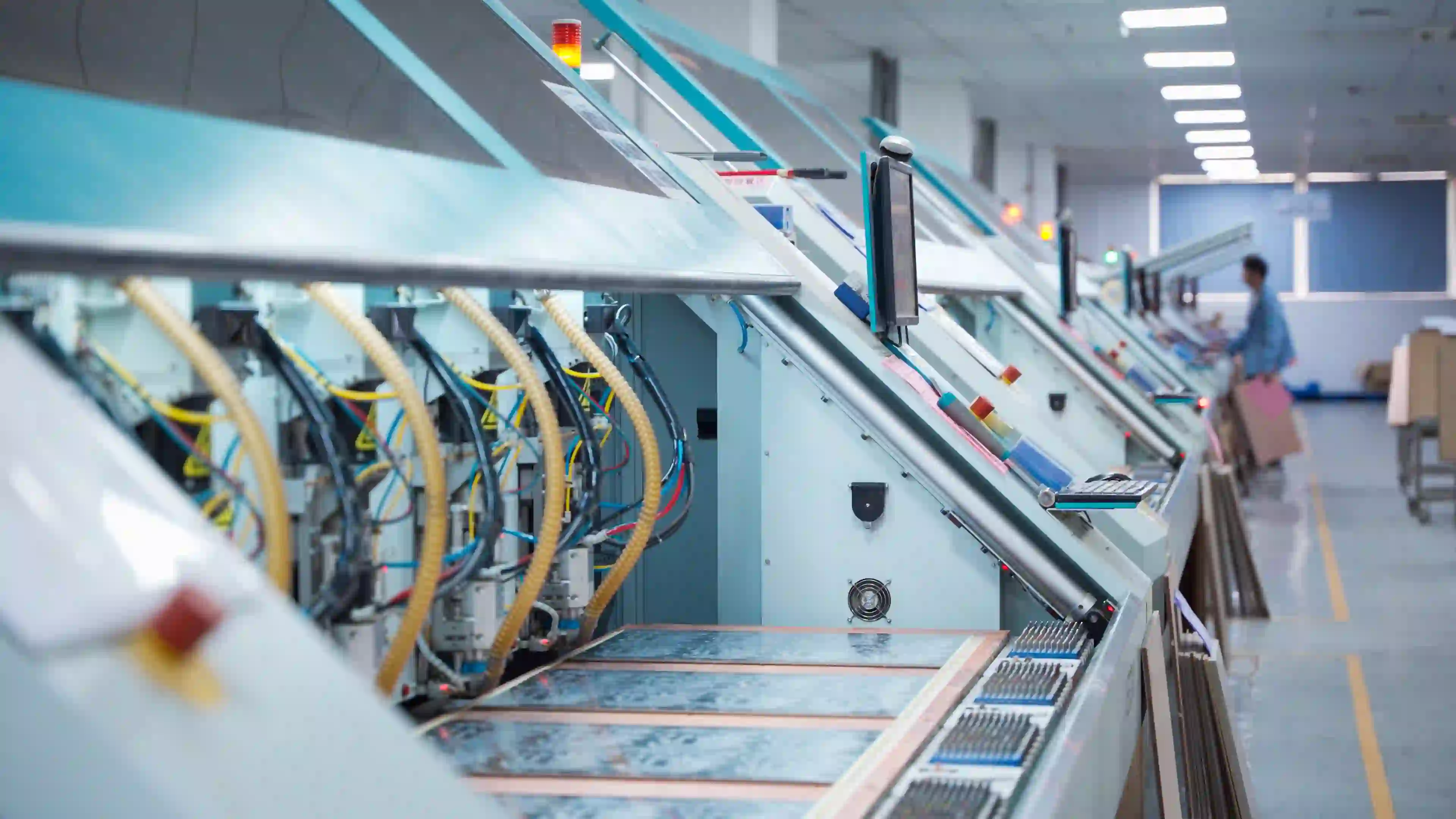
 00:31
00:31
HDI Manufacturing
High-Density Interconnect (HDI) manufacturing represents a critical advancement in printed circuit board (PCB) technology, enabling the creation of compact, high-performance electronics used in everything from smartphones and medical devices to automotive systems and aerospace applications. This tag page on HDI Manufacturing gathers in-depth articles that explore the intricacies of designing and producing these sophisticated boards, which feature finer lines, smaller vias, and multiple layers to support increased component density and faster signal transmission. For engineers, designers, and manufacturers searching for insights into HDI processes, this resource provides essential knowledge on optimizing board layouts to meet stringent performance requirements while minimizing size and weight. Understanding HDI Manufacturing is vital for tackling common challenges such as thermal management, signal integrity, and cost-effective production. Articles here delve into best practices like selecting appropriate substrate materials, implementing microvia technology, and adhering to industry standards such as IPC-2226 for reliable outcomes. Readers can find practical guidance on layer stacking techniques that enhance electrical performance, as well as strategies for integrating blind and buried vias to reduce board footprint without compromising functionality. These insights are particularly useful for professionals aiming to innovate in high-speed computing or IoT devices, where HDI boards offer superior routing density and reduced electromagnetic interference. By browsing the curated content under this tag, you can access case studies and tutorials that illustrate real-world applications, from prototyping to mass production. Whether you are refining your design workflow or troubleshooting manufacturing defects, the articles provide actionable steps to improve efficiency and yield. This collection serves as a comprehensive reference for staying ahead in the evolving field of advanced PCB fabrication.
Video Guide
-
00:31
Technical Articles

Root Causes of PCB Expansion and Shrinkage and How to Mitigate Them

Optimizing PCB Panelization for 8-Layer Production

Why Identical Drill and Pad Sizes Risked Via Failures in a 6-Layer FR4 PCB
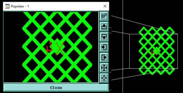
How We Fixed Solder Mask Bridges, Copper Density & Via Issues in Thin 6-Layer HDI PCB
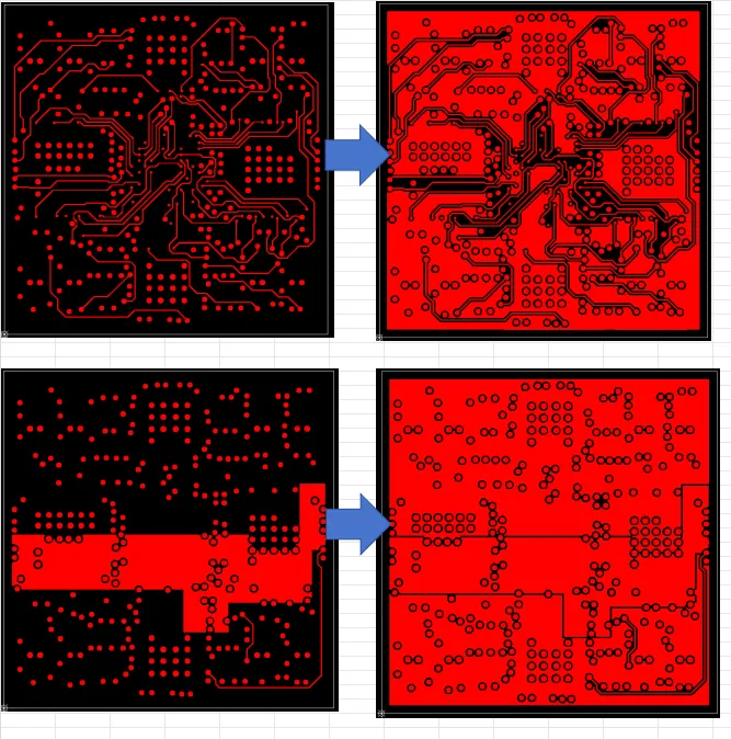
How to Prevent Lamination Failures in 8-Layer HDI PCBs
HDI Manufacturing Process Flow: From Inner Layer to Any-Layer
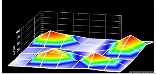
Transverse-Mode Charge-Transfer Capacitive Touch Sensing: Principles, Advantages, and PCB Integration
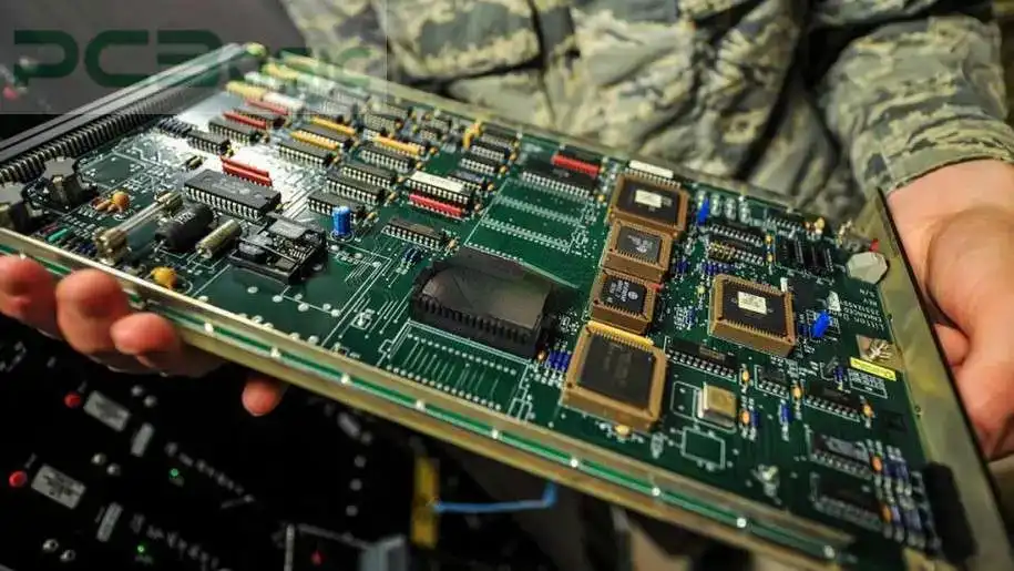
Advanced PCB Manufacturing Techniques for Military Communication Systems
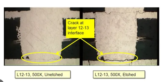
IPC 6012 for HDI PCBs: Addressing Advanced Design Challenges
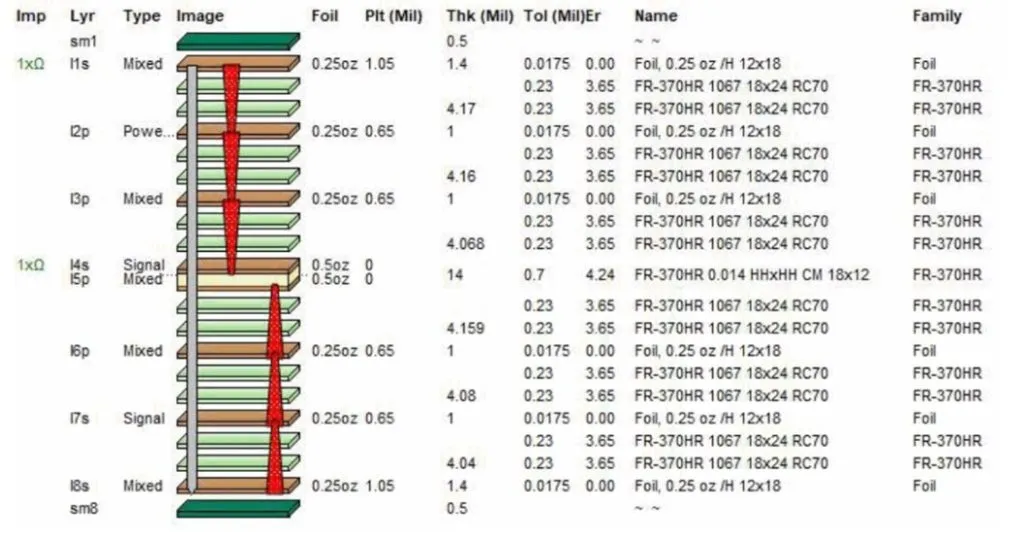
Blind and Buried Vias in Sequential Build Up PCBs: Design and Fabrication Techniques
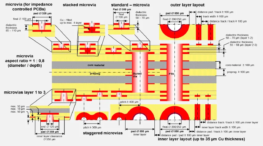
Demystifying Sequential Build Up PCBs: A Beginner's Guide to HDI Technology
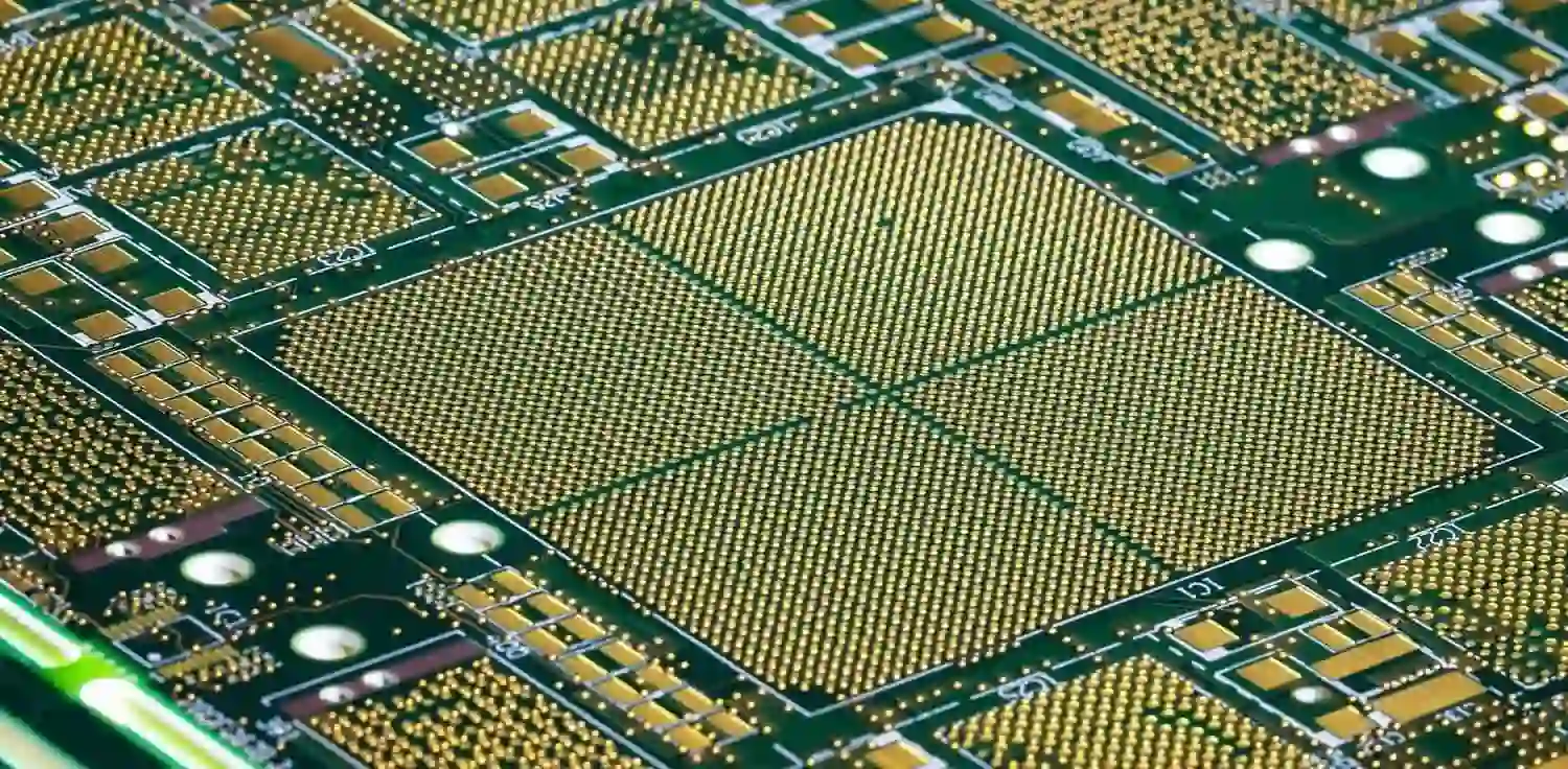
High Density Interconnect (HDI) PCBs in MRI Machines: Advantages and Challenges
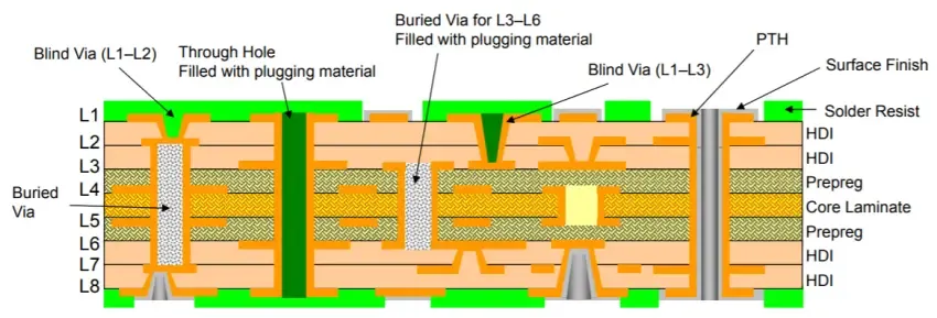
Miniaturized HDI PCB: Design and Manufacturing for Small Form Factor Electronics
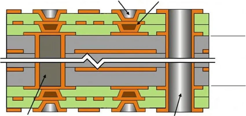
Advanced HDI PCB: Materials, Manufacturing, Design, and Interconnect Technology
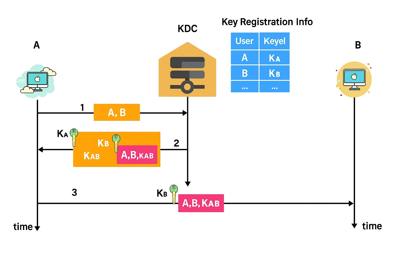
PCB Design and Manufacturing Considerations for Enterprise Firewalls, Network Security Systems, and NAT Traversal Solutions
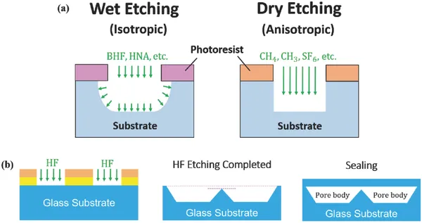
Advanced PCB Etching Techniques for High Density Interconnect (HDI) Boards
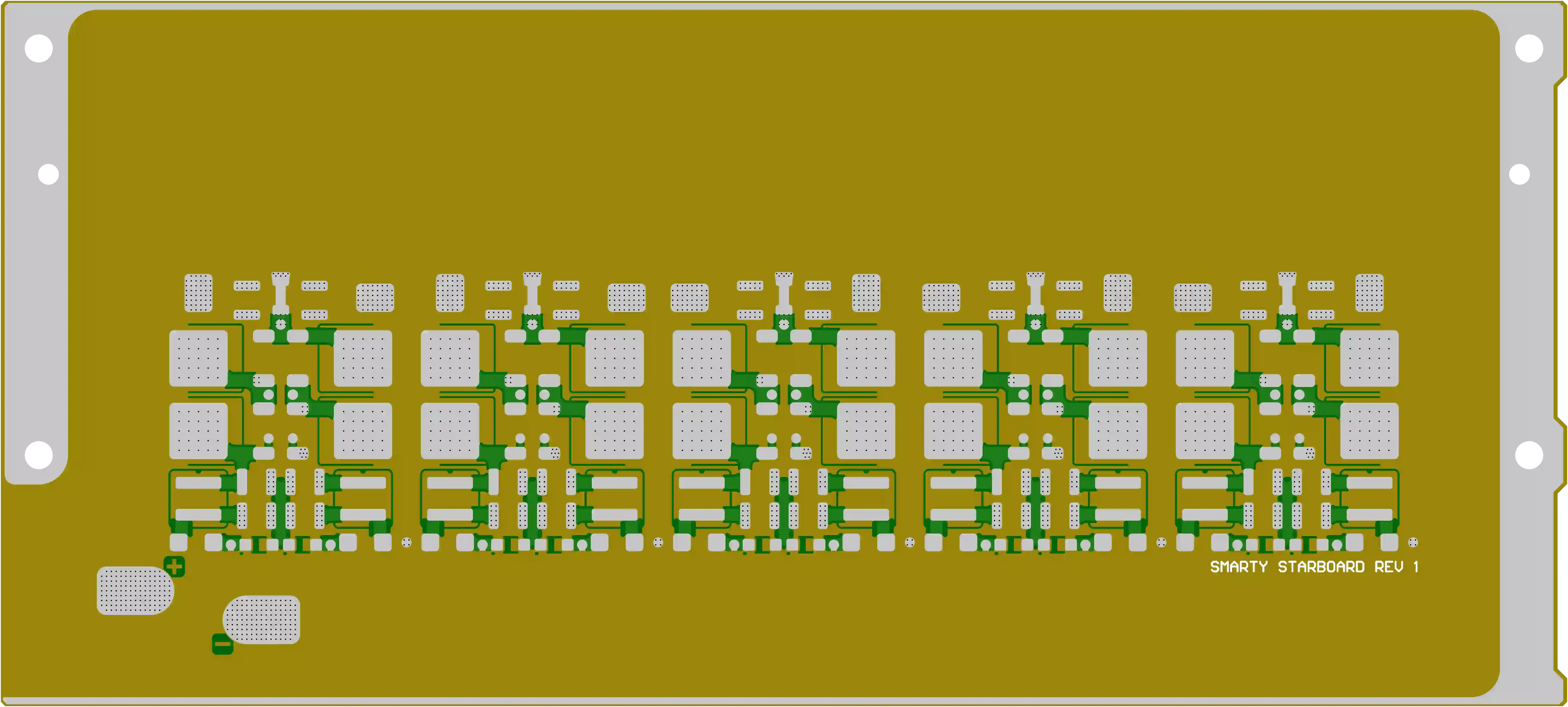
0.15mm Hole & Countersink Depth Control in 4-Layer HDI PCB
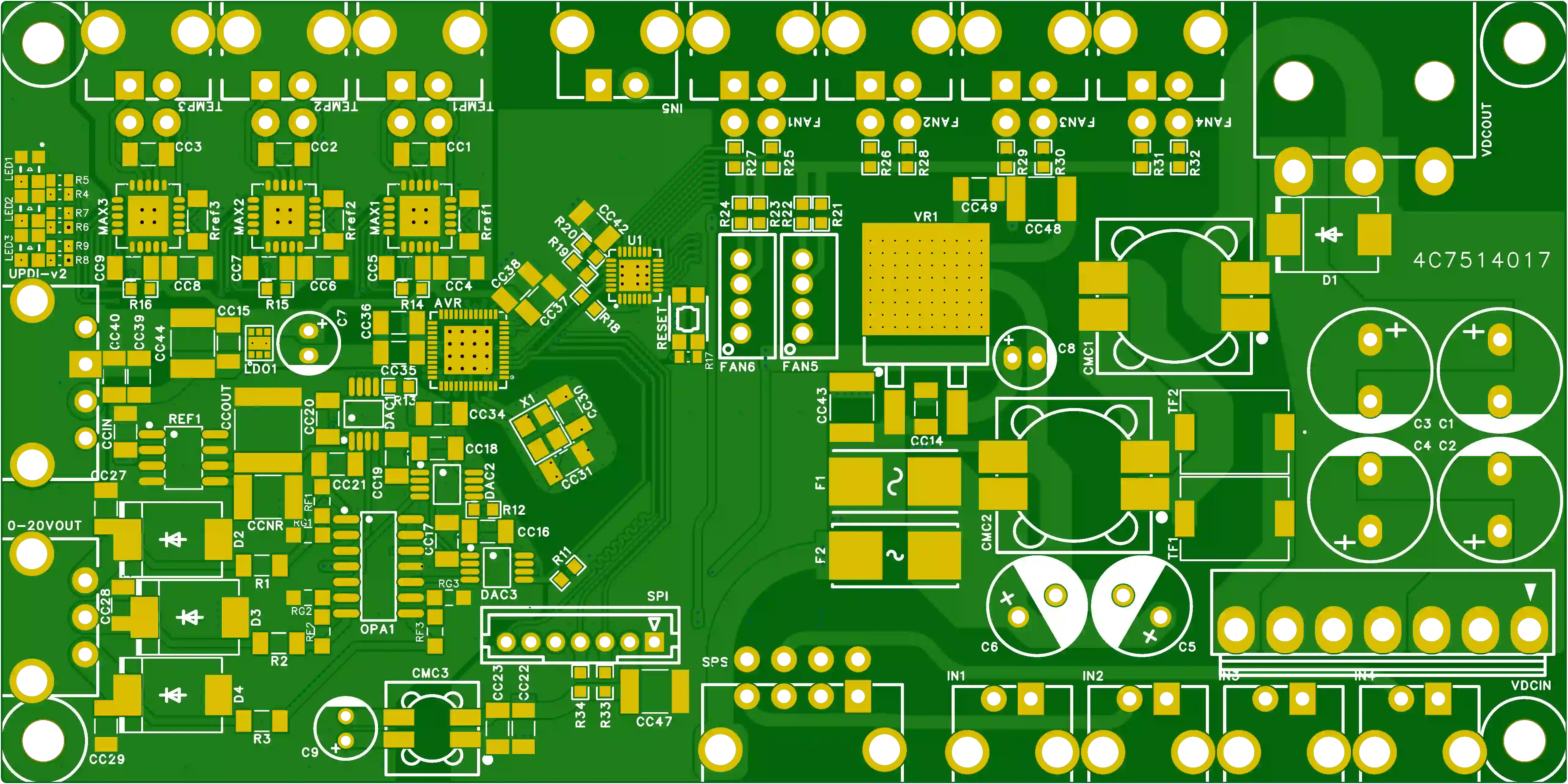
How Conflicting Via Data and Soldermask Definitions Triggered CAM Review in a 4-Layer HDI PCB
How PCB CAM Review Resolves Copper Weight and Panelization EQs on 8-Layer HDI Boards