Introduction
As electronic hobbyists push the boundaries of their projects, the demand for compact, high-performance circuit boards grows. Sequential build-up PCBs, a key part of high-density interconnect (HDI) technology, allow you to pack more components into smaller spaces without sacrificing functionality. These boards are built layer by layer, enabling finer traces and smaller vias that traditional PCBs cannot match. For hobbyists designing drones, wearables, or IoT gadgets, understanding sequential build-up PCB basics opens doors to professional-level miniaturization. This guide breaks down the process, advantages, and applications in simple terms, drawing from factory manufacturing insights. By the end, you will grasp why HDI PCB for beginners like you can elevate your next project.
What Are Sequential Build-Up PCBs and Why Do They Matter?
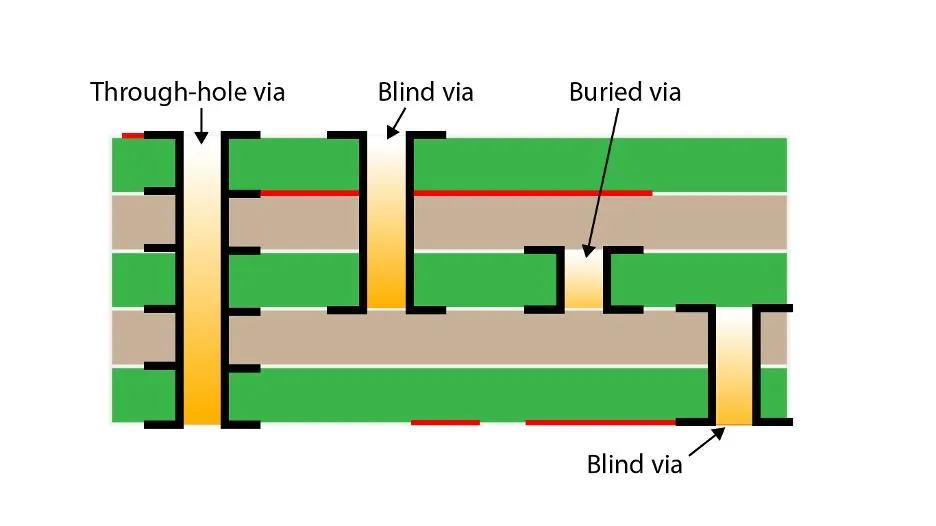
Sequential build-up PCBs, often called SBU boards, form the foundation of HDI technology by constructing multilayer structures through repeated lamination cycles. Unlike standard multilayer PCBs laminated all at once, SBU starts with a central core and adds thin dielectric and copper layers sequentially. This method creates microvias, blind vias, and buried vias that connect layers precisely without spanning the entire board. Hobbyists benefit because these boards support denser routing for complex circuits in tight spaces. In factories, this process aligns with standards like IPC-2226, which outlines design rules for HDI features. As devices shrink, sequential build-up becomes essential for maintaining signal quality and component density.
HDI PCBs matter for hobby projects because they handle fine-pitch components, such as ball grid arrays (BGAs), common in modern microcontrollers and sensors. Traditional boards limit your layout options due to larger via sizes and thicker dielectrics. SBU solves this by enabling stackups like 1+N+1, where N represents core layers and 1 indicates one build-up layer per side. This flexibility reduces board size by up to half in some designs, perfect for portable gadgets. Factories emphasize reliability through controlled lamination, ensuring vias withstand thermal stress. For beginners, grasping these basics means fewer redesigns and better prototypes.
The Technical Principles of Sequential Build-Up
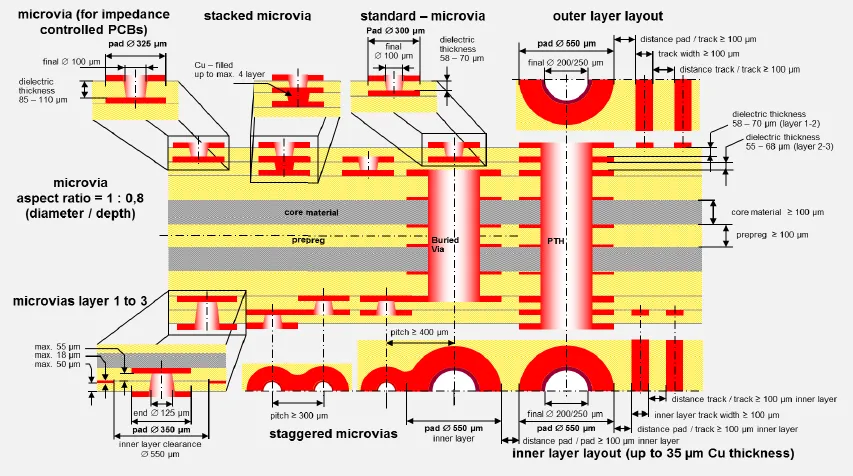
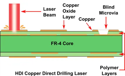
Sequential build-up relies on laser drilling and plating to form microvias with diameters under 150 microns, far smaller than mechanical drills allow. The process begins with fabricating a core, typically 2 to 8 layers, using standard imaging and etching for inner circuits. Thin prepreg sheets and copper foil are then laminated onto this core under heat and pressure, around 250 psi, to bond layers securely. After each lamination, lasers drill blind or buried vias, which are plated with copper to create electrical connections. This cycle repeats, building outward from the core, with each step ensuring alignment via pins for precision. Factories monitor coefficient of thermal expansion (CTE) mismatches to prevent delamination during cooling.
Microvias in SBU boards span just one dielectric layer, keeping aspect ratios low, ideally 0.75:1, for reliable plating. Stacked microvias connect multiple layers by filling and planarizing intermediates, while staggered ones offset for density. Dielectric thicknesses drop to 50-100 microns, supporting trace widths as fine as 75 microns. This layer-by-layer approach contrasts with all-at-once lamination, avoiding warpage in high-layer counts. Per IPC-2226 guidelines, capture pads around 250 microns ensure robust connections. Hobbyists see this as a path to routing high-speed signals without crosstalk in compact designs.
The principles extend to via-in-pad technology, where components sit directly over filled vias, maximizing space. Laser types, like UV or CO2, ablate resin cleanly without damaging copper. Post-drilling, desmear removes residue for plating adhesion. Each cycle adds impedance-controlled traces, vital for hobby RF projects. Standards like IPC-6012 qualify these boards for performance under thermal cycling. Understanding these mechanisms demystifies why SBU excels in density.
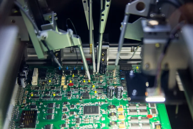
Step-by-Step: How Sequential Build-Up PCBs Are Made
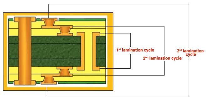
The manufacturing kicks off with inner layer processing: photoresist coats copper-clad laminates, UV exposure defines patterns, and etching reveals traces. The core assembles next, black oxide treated for adhesion, then laminated into subsets. For a 1+N+1 stackup, one cycle laminates outer foils to the core; lasers drill from surface to first inner layer. Vias fill via electroplating, 0.8-1.2 microns thick, followed by outer layer imaging. Additional cycles for 2+N+2 add more subsets, drilling stacked vias precisely. Final steps include solder mask, surface finish, and routing panels into boards.
Quality checks intersperse each phase: electrical testing verifies continuity, X-ray inspects via fill. Sequential cycles, often 2 to 4, depend on via configuration; more cycles mean higher complexity. Alignment pins register layers to microns, countering shrinkage. Cooling solidifies bonds as epoxy cures. This factory-driven sequence ensures HDI reliability. Beginners can visualize it as stacking pancakes, drilling holes, and wiring between.
Post-lamination, outer layers etch fine lines, solder mask protects with 8-mil openings for pads. Impedance tests via time-domain reflectometry confirm 50-ohm lines. For hobbyists ordering prototypes, knowing these steps aids DFM checks. The process scales to 20 layers, but 6-12 suit most projects.
Sequential Build-Up PCB Advantages for Hobbyists
One prime sequential build-up PCB advantage is unmatched routing density, fitting twice the traces versus standard boards. Shorter vias reduce signal delay and loss, ideal for high-speed hobby signals like SPI or USB. Boards shrink overall, enabling palm-sized wearables or drone flight controllers. Microvias support 0.4-mm BGA pitches, unlocking advanced chips. Factories note better thermal management with filled vias acting as heat paths.
Another benefit: superior signal integrity from controlled impedance and low crosstalk. Thin dielectrics minimize stubs, cutting reflections. Reliability improves via staggered vias distributing stress. Cost per density drops for mid-volume runs, accessible for hobby batches. Compared to through-hole vias, SBU cuts inductance by 70 percent in paths. These edges make HDI PCB for beginners worthwhile for performance leaps.
SBU also simplifies escaping dense BGAs, fanning out to inner layers quickly. Warpage control via symmetric stackups keeps boards flat for assembly. Environmentally, thinner materials use less resin. Hobbyists gain professional results without exotic tools.
Sequential Build-Up PCB Applications in Hobbyist Projects
Sequential build-up PCB applications shine in compact IoT sensors, where space constraints demand HDI. Wearables like fitness trackers pack displays, batteries, and Bluetooth into thin profiles using 1+N+1 stacks. Drone electronics benefit from lightweight, high-density boards handling motor drivers and cameras. Medical hobby projects, such as portable monitors, leverage microvias for precise analog routing.
Automotive-inspired gadgets, like dash cams, use SBU for vibration resistance and EMI shielding. 5G experimenters route high-freq signals cleanly. Gaming handhelds or AR glasses employ 2+N+2 for processor-heavy loads. Factories produce these for reliability in harsh conditions. Hobbyists apply them to prototypes scaling to products.
Edge computing nodes in smart homes fit more ports via buried vias. These real-world uses show sequential build-up PCB advantages in action.
Best Practices for Hobbyists Designing with Sequential Build-Up
Start with stackup planning: choose 1+N+1 for simple density, consult fabricator data for materials. Set design rules per IPC-2226: 75-micron lines, 100-micron vias. Place high-density parts centrally, fanout BGAs with microvias. Simulate impedance early to hit 50 ohms. Limit stacked vias to two for reliability.
Symmetrize build-up top and bottom to avoid warpage. Use via-in-pad sparingly, fill and cap them. Space microvias 50 microns center-to-center minimum. Test prototypes electrically before assembly. These practices ensure manufacturability.
Route signals short, ground nearby. Thermal vias under power ICs dissipate heat.
Conclusion
Sequential build-up PCBs demystify HDI for beginners, offering density and performance once reserved for pros. From core lamination to microvia plating, the process delivers compact, reliable boards for hobby innovations. Key advantages like shorter paths and finer features suit drones to wearables. Applications abound in IoT and portables. Follow best practices and standards for success. Dive into sequential build-up PCB basics to supercharge your projects.
FAQs
Q1: What are the sequential build-up PCB basics for a first-time HDI design?
A1: Sequential build-up starts with a core, adds dielectric and copper layers via lamination cycles, and uses laser-drilled microvias for connections. Beginners should opt for 1+N+1 stackups with 2-3 cycles. Focus on fine traces around 75 microns and low aspect ratio vias. Factory alignment ensures precision. This foundation supports hobby prototypes reliably.
Q2: Why choose HDI PCB for beginners in compact electronics?
A2: HDI PCB for beginners enables smaller boards with higher component counts, perfect for wearables or drones. Microvias reduce signal paths, improving speed over standard PCBs. It handles fine-pitch parts easily. Start simple to learn stackups. Benefits outweigh learning curve for dense layouts.
Q3: What are the main sequential build-up PCB advantages over traditional boards?
A3: Sequential build-up PCB advantages include double the routing density, better signal integrity from short vias, and smaller overall size. It supports high-speed signals with controlled impedance. Reliability rises via staggered structures. Ideal for hobby high-performance needs. Factories confirm thermal benefits too.
Q4: Where are sequential build-up PCB applications most useful for hobbyists?
A4: Sequential build-up PCB applications thrive in IoT sensors, wearables, and drones needing compactness. They route dense BGAs in gaming devices or edge computers. Medical prototypes gain precision. High-freq experiments like 5G use them for low loss. Versatile for innovative projects.
References
IPC-2226A - Sectional Design Standard for High Density Interconnect (HDI) Printed Boards. IPC, 2017
IPC-6012E - Qualification and Performance Specification for Rigid Printed Boards. IPC, 2017
IPC-6016E - Qualification and Performance Specification for High Density Interconnect (HDI) Printed Boards. IPC, 2020