Introduction
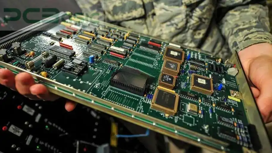
Military communication systems demand printed circuit boards (PCBs) that deliver exceptional reliability under extreme conditions, including high vibration, temperature fluctuations, and electromagnetic interference. Advanced manufacturing techniques enable the production of high-density interconnect (HDI) PCBs essential for compact, high-performance devices like radios, satellite links, and secure data transceivers. These methods address challenges in signal integrity, miniaturization, and long-term durability critical for mission-critical applications. Techniques such as laser direct imaging (LDI), microvia formation, sequential lamination, fine-line etching, and optimized surface finish play pivotal roles in achieving these goals. Factory processes must align with rigorous quality controls to ensure PCBs withstand operational stresses without failure. This article explores these techniques from a manufacturing perspective, providing insights for electrical engineers designing or procuring such boards.
The Imperative for Advanced PCB Techniques in Military Applications
Military communication systems prioritize size, weight, and power (SWaP) optimization alongside unwavering reliability. Traditional PCB fabrication struggles with the dense routing and interlayer connections required for high-frequency signals in modern tactical networks. Advanced techniques allow for tighter trace spacing, smaller vias, and multilayer builds that maintain electrical performance in harsh environments. Compliance with standards like IPC-6012DS ensures qualification for space and military avionics, emphasizing vibration resistance and thermal cycling endurance. These methods reduce parasitic inductance and capacitance, preserving signal integrity for data rates exceeding gigabits per second. Manufacturers focus on process repeatability to meet these demands consistently across production runs.
Laser Direct Imaging (LDI): Precision Patterning for High-Density Features
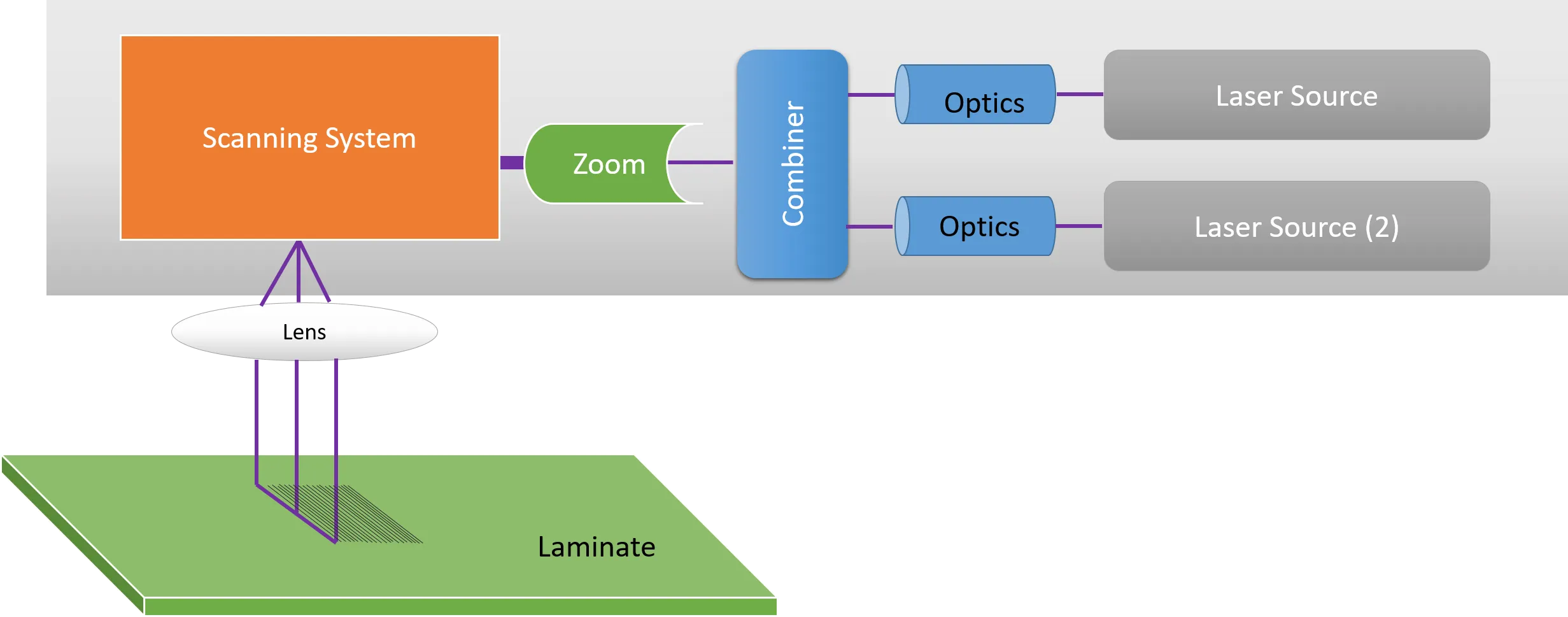
Laser direct imaging (LDI) revolutionizes PCB patterning by projecting digital images directly onto photosensitive dry films using a controlled laser beam, eliminating traditional phototools prone to distortion. This contactless process achieves superior resolution for fine features, crucial in military systems where trace widths must support high-speed signals without crosstalk. LDI excels in multilayer boards, allowing adjustments for registration errors during sequential builds. Factories implement LDI to handle complex geometries, reducing defects like over-etching or under-exposure common in conventional lithography. The technique supports aspect ratios that enhance yield in production. For military communications, LDI ensures patterns align precisely across layers, vital for impedance-controlled transmission lines.
In practice, LDI systems scan the board surface in a raster pattern, exposing only necessary areas for efficiency. This minimizes waste and enables rapid prototyping iterations during design validation. Engineers benefit from its flexibility in handling panel sizes and curvatures that occur in rigid-flex hybrids used in portable devices. Post-exposure development follows standard chemical processes, but LDI's precision upstream improves downstream etching outcomes. Manufacturers calibrate lasers for wavelength compatibility with various photoresists, optimizing exposure doses. Overall, LDI sets the foundation for subsequent advanced steps like fine-line etching.
Microvia Formation: Enabling Interlayer Connectivity in HDI Structures
Microvia formation employs laser ablation to create small-diameter vias, typically connecting adjacent layers in HDI PCBs for military communication modules. UV or CO2 lasers vaporize dielectric material precisely, forming vias with smooth walls that facilitate reliable plating. This technique supports buildup structures where space constraints demand vertical interconnects without consuming surface routing area. Factories desmear vias post-drilling to remove residue, ensuring void-free copper fill during electroplating. Microvias reduce signal path lengths, minimizing latency in real-time data links. Sequential integration with lamination cycles allows multiple microvia generations in a single board.
The choice of laser type depends on material ablation rates; UV lasers handle finer features in advanced dielectrics. Post-formation, vias undergo cleaning and plating to achieve IPC-compliant barrel quality. In military applications, these vias endure mechanical stresses from shock and vibration. Manufacturers inspect via geometry using automated optical systems for annulus and taper control. This process integrates seamlessly with fine-line patterning, enabling denser component placement. Reliable microvia formation directly impacts overall board yield and field performance.
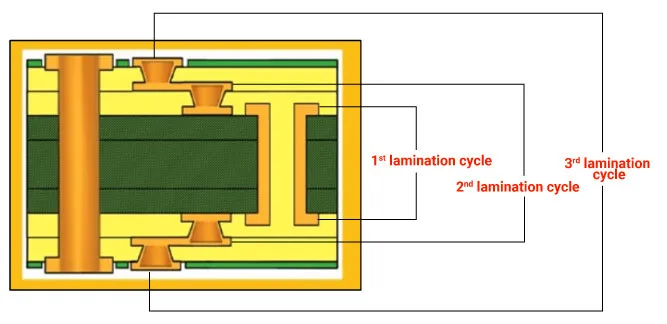
Sequential Lamination: Building Multilayer HDI Configurations
Sequential lamination constructs HDI PCBs by iteratively laminating cores and prepregs, incorporating microvias between each cycle for enhanced density. Unlike all-at-once lamination, this method builds layers incrementally, allowing blind and buried vias tailored to signal routing needs. Factories control press parameters like temperature ramps and pressure to prevent warpage in thin multilayers common in communication antennas. Each cycle includes via formation, filling, and patterning before the next lamination, ensuring interlayer alignment. This approach suits military systems requiring 10+ layers with mixed high-speed and power planes. Standards such as IPC-2226 guide design parameters for these structures, focusing on reliability under thermal stress.
Process control during sequential lamination mitigates resin flow issues that could bridge fine features. Engineers specify buildup types like 1+n+1 or 2+n+2 based on via fanout and density. Post-lamination, boards undergo baking to stabilize dimensions before final processing. Factories employ fiducials for registration accuracy across cycles. This technique enables embedded components for further SWaP reduction in secure transceivers. Sequential lamination thus forms the backbone of complex military PCB architectures.
Fine-Line Etching: Achieving Trace Precision for Signal Integrity
Fine-line etching patterns conductors with minimal linewidth and spacing, essential for high-frequency military communication circuits prone to crosstalk and loss. Plasma or chemical etchants remove unprotected copper selectively, with LDI masks enabling sub-50-micron features. Factories optimize etch rates and conveyor speeds to maintain sidewall profiles perpendicular to the board. Tent-and-etch or etch-back processes prevent undercutting, preserving critical dimensions. This technique pairs with microvias to route dense differential pairs for RF signals. Uniform etch factors ensure impedance consistency across the panel.
Advanced etching integrates with surface preparation to avoid haloing around pads. Manufacturers use endpoint detection to halt etching precisely, reducing variability. In military contexts, fine lines support higher pin counts in FPGAs and ASICs for processing encrypted data. Post-etch inspection verifies spacing using electrical test probes. Fine-line etching thus upholds the electrical performance demanded by tactical networks.
Surface Finish Selection: Ensuring Long-Term Solderability and Protection
Surface finish protects exposed copper from oxidation while enabling reliable soldering and wire bonding in military assemblies. Options like electroless nickel immersion gold (ENIG) provide flat, uniform coverage ideal for fine-pitch components in communication modules. Immersion tin or organic solderability preservatives (OSP) offer alternatives based on assembly methods and shelf life needs. Factories apply finishes post-etching and routing, controlling thickness for black pad avoidance. For harsh environments, hard gold variants enhance wear resistance in edge connectors. J-STD-001 guidelines dictate finish acceptance for high-reliability class 3 products.
Compatibility with sequential processes ensures no degradation during multiple thermal exposures. Engineers select finishes balancing cost, contact resistance, and RoHS compliance. Testing verifies whisker growth prevention in tin finishes. Surface finish completes the manufacturing chain, safeguarding functionality over extended deployments.
Best Practices for Integrating These Techniques in Production
Integrate laser direct imaging (LDI) early to define patterns accurately before microvia formation and sequential lamination. Maintain cleanroom conditions to prevent contamination during fine-line etching and surface finish application. Use design for manufacturability (DFM) rules from IPC-2226 to optimize via stacking and trace routing. Factories implement statistical process control for yield monitoring across cycles. Validate prototypes with cross-section analysis and thermal cycling tests. Collaboration between design and manufacturing teams ensures alignment with military qualification flows.
Conclusion
Advanced PCB manufacturing techniques like laser direct imaging (LDI), microvia formation, sequential lamination, fine-line etching, and surface finish enable military communication systems to achieve superior density and reliability. These processes, grounded in factory expertise and standards compliance, address the unique challenges of miniaturization and environmental resilience. Electrical engineers can leverage these insights to specify boards that perform flawlessly in the field. Prioritizing process control and integration maximizes production efficiency and product lifespan. As demands for faster, smaller systems grow, mastering these techniques remains essential for defense electronics.
FAQs
Q1: What role does laser direct imaging (LDI) play in military PCB manufacturing?
A1: Laser direct imaging (LDI) provides precise digital patterning without phototools, ideal for fine features in high-density military communication PCBs. It reduces alignment errors in multilayer builds and supports rapid adjustments for design changes. Factories use LDI to achieve consistent results across panels, enhancing yield for sequential processes. This technique aligns with IPC quality requirements for high-reliability applications.
Q2: How does sequential lamination benefit microvia formation in HDI PCBs?
A2: Sequential lamination allows iterative buildup with microvia formation between layers, enabling complex HDI structures for compact military systems. It facilitates blind and buried vias that shorten signal paths and improve integrity. Manufacturers control thermal profiles to minimize warpage during cycles. This method supports higher layer counts essential for advanced communication routing.
Q3: Why is fine-line etching critical for surface finish in military applications?
A3: Fine-line etching creates precise traces before surface finish application, ensuring solderability and protection in dense layouts. It prevents issues like bridging in high-vibration environments. Factories optimize etchants for uniform copper removal, complementing finishes like ENIG. This combination upholds signal performance over long missions.
Q4: What standards guide surface finish selection for military PCBs?
A4: Standards like J-STD-001 specify acceptability for surface finishes in class 3 assemblies used in military communications. They address solder joint reliability and environmental resistance. Engineers select based on assembly processes and contact needs. Factory processes ensure compliance through thickness control and testing.
References
IPC-6012DS — Space and Military Avionics Applications Addendum to IPC-6012D. IPC
IPC-2226 — Design Standard for High Density Interconnect (HDI). IPC
J-STD-001 — Requirements for Soldered Electrical and Electronic Assemblies. IPC


