Introduction
Sequential build-up PCBs represent a cornerstone in modern high-density interconnect technology, enabling compact designs for advanced electronics. Blind vias sequential build-up and buried vias sequential build-up allow connections between specific layers without penetrating the entire board thickness, optimizing routing space and reducing signal path lengths. These vias address the limitations of traditional through-hole vias in multilayer boards, where density demands exceed standard capabilities. Electrical engineers rely on precise via design sequential build-up to ensure signal integrity, thermal performance, and manufacturability. This article explores the design principles and fabrication methods that make these vias reliable in sequential build-up processes. Factory insights reveal how these techniques balance complexity with yield.
Understanding Blind and Buried Vias in Sequential Build-Up PCBs
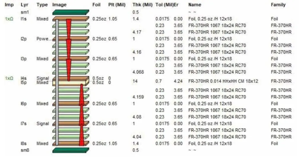
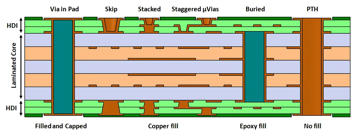
Blind vias connect an outer layer to an immediate inner layer, stopping short of the opposite side, while buried vias link two or more internal layers entirely within the board. In sequential build-up, these vias form through iterative lamination cycles, contrasting with all-at-once drilling in standard multilayers. This layered approach supports higher interconnect densities essential for applications like smartphones and automotive electronics. Through vias waste inner layer space, but blind and buried vias sequential build-up free up real estate for traces and components. Engineers must consider via types during stackup planning to avoid routing congestion. The sequential nature demands careful sequencing to align vias across build cycles.
Why Blind and Buried Vias Matter in Sequential Build-Up
These vias enable finer pitch routing and shorter signal paths, minimizing inductance and crosstalk in high-speed designs. Sequential build-up PCBs with blind vias sequential build-up achieve HDI-like performance without full microvia processes, controlling costs for mid-range densities. Buried vias sequential build-up further densify inner layers, supporting complex power distribution networks. From a manufacturing view, they reduce board thickness while maintaining structural integrity. Electrical engineers benefit from improved impedance control and reduced electromagnetic interference. Ultimately, these vias drive miniaturization without sacrificing reliability.
Design Techniques for Blind and Buried Vias
Via design sequential build-up starts with stackup definition, specifying core thickness and build-up layers to accommodate via spans. Engineers position blind vias near component pads for direct fanout, staggering them to prevent overlap in adjacent cycles. Buried vias require pre-planning in core sections, ensuring alignment fiducials guide subsequent laminations. Aspect ratios must stay within manufacturable limits to facilitate plating uniformity. Pad annular rings provide sufficient landing areas for traces, preventing breakout failures. Software stackup tools verify via spans against layer counts, flagging potential conflicts early.
Considerations include thermal expansion matching between dielectrics and copper to avoid via cracking under stress. Signal layers adjacent to power planes benefit from buried vias for shielding. Factory-driven design rules emphasize non-overlapping via fields to simplify drilling sequences. Electrical engineers optimize via placement for current carrying capacity, spacing them adequately from edges. Iterative simulations predict via reliability under operational loads.
IPC-2226 provides guidelines for HDI structures incorporating these vias, emphasizing construction classes.
Fabrication Techniques in Sequential Build-Up
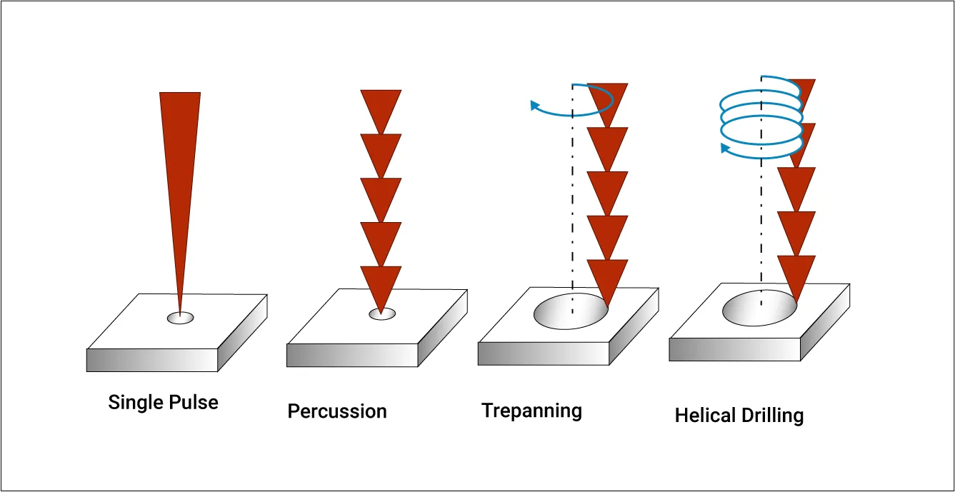
Sequential build-up begins with a central core, often 2- or 4-layer, featuring buried vias drilled and plated first. Additional dielectric and copper foils laminate onto both sides, followed by imaging, etching, and drilling for the next via tier. Blind vias sequential build-up use laser ablation for precision in thin dielectrics, removing resin selectively without damaging inner copper. Mechanical drilling suits larger buried vias in thicker cores. Post-drill desmear ensures clean walls for plating adhesion.
Electroplating fills or lines vias with copper, building tenting over pads for planar surfaces. Via filling sequential build-up employs conductive or non-conductive pastes for stacked configurations, preventing voids during lamination. Multiple cycles repeat until the full stack achieves, with outer layers patterned last. Plasma cleaning enhances surface activation between steps. Quality checks like cross-sectioning verify fill completeness.
Buried vias form entirely within sub-stacks, plated before outer build-ups encapsulate them. This factory process demands tight registration tolerances.
Via Filling Methods in Sequential Build-Up
Via filling sequential build-up ensures flat surfaces for fine-line imaging, critical for density. Electroplated copper fully fills vias in high-current applications, offering low resistance paths. Non-conductive fills like epoxy resins cap blind vias, supporting via-in-pad designs. Conductive pastes screen-print into vias before plating, aiding thermal dissipation. Selection depends on stackup complexity and reliability needs.
Filling follows plating, with electroforming for deep vias to achieve void-free structures. Capping layers planarize the surface, enabling trace widths under 50 microns. Factory processes screen for fill density via X-ray inspection. Electrical engineers specify fill types based on signal speed and power demands. These methods mitigate electromigration in high-frequency vias.
Best Practices for Reliable Implementation
Adhere to staggered via configurations over stacked to ease alignment and reduce stress concentrations. Maintain symmetric build-up to prevent warpage, balancing copper distribution across layers. IPC-6012 outlines plating thickness requirements for via integrity, ensuring durability. Simulate thermomechanical stress during design to predict failures. Limit via density per layer to sustain yields.
Collaborate with fabricators early for process capabilities, adjusting designs iteratively. Use fiducials extensively for registration in multi-cycle builds. Post-fab electrical testing verifies continuity and isolation. These practices align factory output with engineering intent.
Challenges and Troubleshooting Insights
Alignment shifts in sequential lamination cause open vias, addressed by enhanced fiducial patterns and optical registration. Plating voids from poor desmear lead to reliability issues, mitigated by optimized chemistry. Warpage from asymmetric stacks requires controlled lamination pressures. Factory data shows via cracking under thermal cycling stems from CTE mismatch, resolved by resin selection. Electrical engineers troubleshoot via resonance with TDR measurements.
Conclusion
Blind vias sequential build-up and buried vias sequential build-up unlock higher densities in sequential build-up PCBs through meticulous design and fabrication. Via design sequential build-up and via filling sequential build-up ensure performance in demanding applications. Standards like IPC-2226 and IPC-6012 guide these processes toward robustness. Electrical engineers gain compact, reliable boards by integrating factory insights. Future advancements will refine these techniques for even tighter pitches.
FAQs
Q1: What distinguishes blind vias sequential build-up from buried vias sequential build-up?
A1: Blind vias connect outer to inner layers, visible from one surface, while buried vias link internal layers only, hidden entirely. Sequential build-up fabricates them via iterative cycles, with blind vias drilled post-lamination and buried in cores. This enables dense routing without through-hole interference. Factory processes prioritize alignment for both.
Q2: How does via design sequential build-up impact signal integrity?
A2: Optimal stackup planning shortens via stubs, reducing inductance in high-speed signals. Staggered placements minimize crosstalk between vias. Engineers balance density with spacing for impedance control. Sequential build-up supports finer geometries, enhancing overall performance.
Q3: What are common via filling sequential build-up methods?
A3: Electroplating achieves full copper fills for conductivity, while epoxy pastes cap for planarity. Conductive fills suit power vias, non-conductive for signals. Factory selection depends on stackup and reliability tests. These ensure void-free structures post-lamination.
Q4: Why reference standards like IPC in blind and buried via fabrication?
A4: IPC-2226 defines HDI classes for via configurations, ensuring design feasibility. IPC-6012 specifies plating and qualification, aligning factory output with quality. Electrical engineers use them for compliant, reliable sequential build-up PCBs.
References
IPC-2226 — Sectional Design Standard for High Density Interconnect (HDI) Printed Boards. IPC.
IPC-6012E — Qualification and Performance Specification for Rigid Printed Boards. IPC, 2017.
IPC-A-600K — Acceptability of Printed Boards. IPC, 2020.


