Introduction
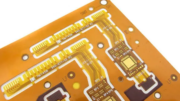
HDI PCB represents a transformative technology in electronics manufacturing. High-Density Interconnect printed circuit boards enable engineers to pack significantly more functionality into smaller spaces while delivering superior electrical performance, thermal management, and long-term reliability.
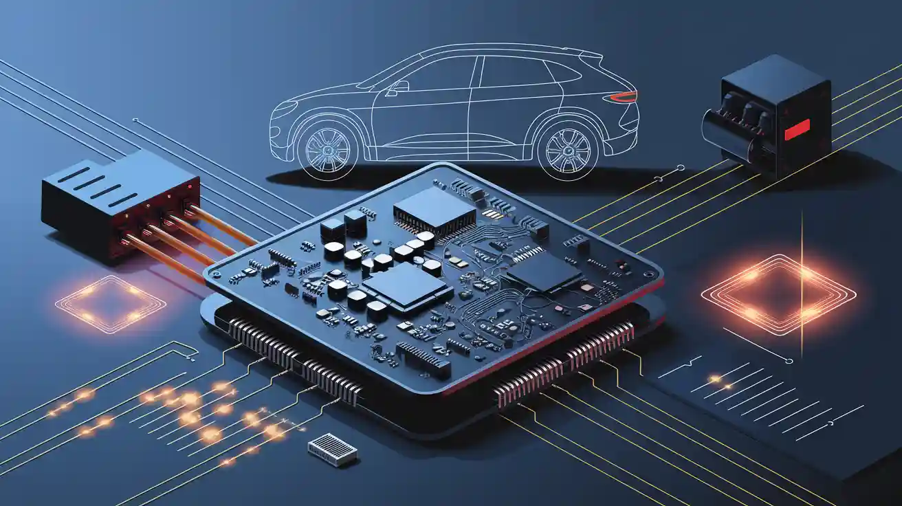
Today's electronic devices—from smartphones and wearable medical sensors to 5G base stations, autonomous vehicles, and industrial IoT modules—rely on HDI PCB to meet strict miniaturization and speed requirements. Compared with traditional PCBs, HDI technology typically reduces board size by 30–50%, shortens signal paths, lowers power consumption, and supports finer-pitch components such as 0.3 mm BGAs.
This comprehensive guide provides a clear overview of what HDI PCB is, why it has become essential, and how its four core pillars—HDI PCB Design, HDI PCB Manufacturing, HDI PCB Assembly, and HDI PCB Application—work together to deliver high-performance results.
What Is HDI PCB and Why It Matters
HDI PCB uses microvias, fine traces, sequential lamination, and advanced materials to achieve wiring densities far beyond standard FR-4 boards. Microvias as small as 0.075 mm connect layers without penetrating the entire board, allowing designers to route hundreds of signals under a single BGA package.
The technology delivers measurable advantages:
- Smaller form factors for wearables and medical implants
- Higher signal integrity at multi-gigahertz frequencies
- Better thermal dissipation through dense copper structures
- Reduced weight and material usage
- Support for high I/O count components
As electronics continue to shrink while performance demands rise, HDI PCB has evolved from a specialized technique into a mainstream requirement across consumer, automotive, aerospace, and medical industries.
HDI PCB Design
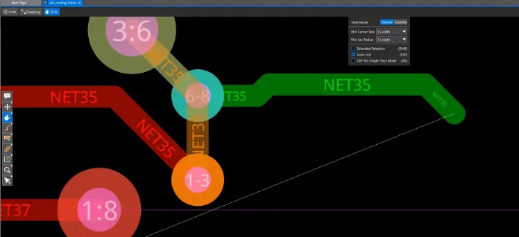
HDI PCB Design forms the foundation of every successful high-density board. It involves selecting the appropriate HDI type (1-step, 2-step, or any-layer), planning symmetric stack-ups, choosing microvia diameters, and optimizing trace routing for signal integrity.
Key design considerations include maintaining aspect ratios below 0.8:1, using via-in-pad technology, applying length-matched differential pairs, and dedicating inner layers to power and ground planes. Designers must also perform thorough impedance control and thermal simulation before releasing artwork.
Professionals who master HDI PCB Design can create boards with 500+ nets per square centimeter while meeting strict EMI and crosstalk limits.
HDI PCB Manufacturing
HDI PCB Manufacturing transforms design files into functional boards through a series of precision processes. The workflow begins with material selection and includes laser drilling of microvias, desmear and electroless copper deposition, semi-additive or modified semi-additive etching for fine lines under 50 µm, sequential lamination, via filling, and final surface finish application.
Critical innovations in this stage include vacuum-assisted via filling, AI-driven real-time process monitoring, and advanced etching techniques that maintain yield above 98%. Strict process controls ensure boards survive 1,000+ thermal cycles and meet IPC-6012E Class 3 requirements.
HDI PCB Manufacturing demands tight tolerances and specialized equipment that standard PCB lines often cannot provide.
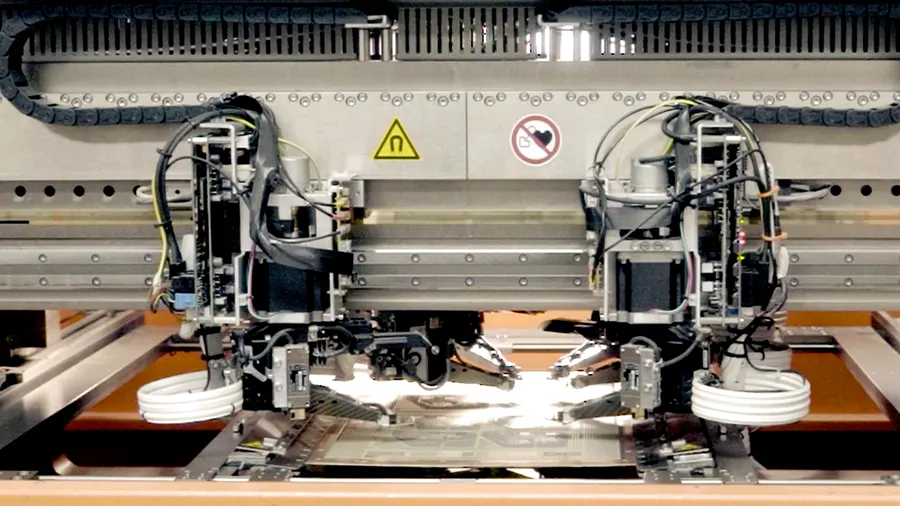
HDI PCB Assembly
HDI PCB Assembly requires specialized techniques because of the dense component placement and delicate microvia structures. Reflow soldering profiles must be carefully controlled to avoid damaging fine traces or filled vias. Via-in-pad designs often need conductive or non-conductive via plugging before component placement.
Best practices for HDI PCB Assembly include:
- X-ray inspection of every hidden joint and via
- Selective soldering or laser soldering for fine-pitch parts
- Careful handling to prevent mechanical stress on thin cores
- Post-assembly thermal cycling and electrical testing
Successful HDI PCB Assembly directly determines the final yield and field reliability of the finished product.
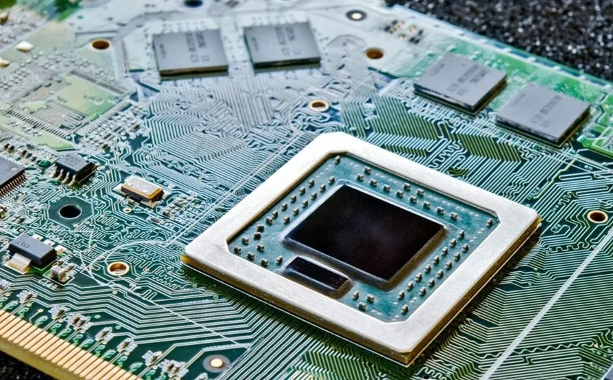
HDI PCB Application
HDI PCB Application spans virtually every modern industry that demands miniaturization and high performance. In consumer electronics, HDI enables slim smartphones and smartwatches. In medical devices, it supports implantable sensors and portable diagnostic equipment. Automotive and 5G infrastructure use HDI for radar modules and small-cell antennas. Aerospace and defense applications benefit from the technology's weight savings and reliability under extreme conditions.
Each HDI PCB Application requires tailored material choices, stack-up strategies, and qualification testing to match specific environmental and electrical demands.
Comparing HDI PCB with Standard PCB Technology
Standard PCBs typically use through-hole vias and 4–8 mil trace/space on FR-4. HDI boards use laser-drilled microvias, sequential build-up layers, and advanced laminates, achieving 3–5 times higher routing density. The result is smaller boards, faster signals, and greater design flexibility.
While standard boards remain suitable for simple or low-volume projects, HDI PCB becomes the clear choice once component pitch drops below 0.65 mm or signal frequencies exceed 1 GHz.
Real-World Impact and Benefits
Companies that adopt HDI PCB consistently report:
- 40–60% reduction in board area
- 20–30% improvement in signal speed
- Lower power consumption due to shorter traces
- Higher reliability from better thermal management
These benefits translate into smaller end products, longer battery life, and faster time-to-market.
Future Trends in HDI PCB Technology
The future of HDI PCB points toward even finer features. Sub-20 µm lines, any-layer microvia structures, and hybrid integration with fan-out wafer-level packaging are already entering production. Sustainable low-loss materials and AI-optimized manufacturing processes will further improve yield and environmental performance. By 2030, 6G devices and advanced AI accelerators are expected to rely heavily on these next-generation HDI capabilities.
Conclusion
HDI PCB technology continues to redefine what is possible in electronics. By mastering HDI PCB Design, optimizing HDI PCB Manufacturing, executing reliable HDI PCB Assembly, and targeting the right HDI PCB Application, engineers and manufacturers can create smaller, faster, and more reliable products that meet today’s demanding requirements. This guide has provided a complete overview of the technology and its four interconnected pillars. Whether you are starting your first HDI project or scaling production, the knowledge shared here will help you navigate every stage with confidence and achieve superior results.