In today’s electronics industry, where miniaturization, high-speed performance, and reliability are non-negotiable, HDI PCB assembly has become a critical technology. High-Density Interconnect (HDI) PCB assembly enables designers to achieve greater component density, superior signal integrity, better thermal management, and smaller form factors than traditional multilayer PCBs.
HDI PCB assembly encompasses the entire process — from material selection and stack-up design through fabrication, component placement, soldering, inspection, and testing. This HDI PCB guide highlights how the process relies heavily on microvias, blind and buried vias, sequential lamination, fine-line routing, and carefully chosen advanced materials.
What Is HDI PCB Assembly and Why It Matters
HDI PCB assembly is the specialized process of building and assembling boards that use microvias (typically ≤ 0.15 mm), finer traces and spaces (often 2–4 mils), and advanced build-up constructions to achieve significantly higher interconnection density than standard PCBs.
Compared with conventional boards, HDI assembly offers:
- Smaller board size and reduced weight
- Improved signal integrity for high-speed designs
- Better power integrity and lower EMI
- Enhanced thermal dissipation in dense layouts
- Support for fine-pitch components (BGA, μBGA, 01005)
However, these benefits require precise control over materials, stack-up configuration, via structures, and design rules. Poor decisions in any of these areas can lead to warpage, plating voids, signal degradation, assembly defects, or field failures.
Success in HDI PCB assembly rests on three foundational pillars: intelligent material selection, optimized stack-up design, and rigorous DFM — topics explored in depth in our dedicated cluster pages.
HDI Assembly Stack-Up Structures and Materials: Building the Foundation
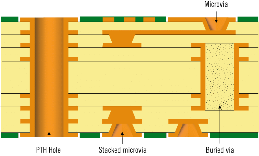
HDI assembly stack-up structures and materials form the physical and electrical backbone of any successful project. Common build-up types include 1+N+1, 2+N+2, and higher-order constructions (3+N+3 or any-layer HDI). Each configuration offers different trade-offs between routing density, cost, reliability, and thermal performance.
Via structures — microvias, blind vias, buried vias, stacked microvias, staggered microvias, and via-in-pad — must be chosen according to density requirements, signal integrity needs, and plating capability. Symmetry in the stack-up is essential to minimize warpage during lamination and reflow soldering. Copper distribution, dielectric thickness, and material properties should be balanced on both sides of the board.
Material selection directly influences the viability of the chosen stack-up. Designers should prioritize laminates with stable dielectric constant (Dk), low dissipation factor (Df), high glass transition temperature (Tg > 170°C), well-matched CTE, and appropriate thermal conductivity. Prepreg flow characteristics and copper foil type (ED vs RA, standard vs low-profile) must also be considered for fine-line etching and reliable microvia plating.
For a detailed breakdown of popular HDI build-up configurations, via reliability considerations, copper weights, and real-world stack-up examples, please refer to our cluster article: HDI assembly stack-up structures and materials.
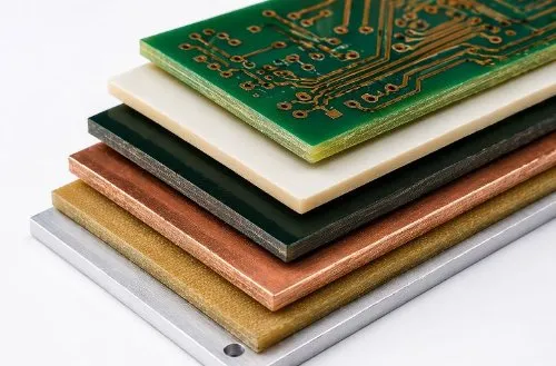
Selecting the Right Materials for HDI PCB Assembly
Selecting the right materials for HDI PCB assembly is one of the most impactful decisions in the entire project. Material properties affect signal loss, impedance control, thermal performance, reliability under thermal cycling, moisture absorption, and overall assembly yield.
Key parameters to evaluate include Dk, Df, Tg, Td, CTE (x, y, z), thermal conductivity, and resin chemistry (standard FR-4 epoxy, high-Tg epoxy, polyimide, hydrocarbon, PTFE, or ceramic-filled systems). Copper foil roughness also matters significantly for high-frequency applications due to skin effect.
Best practices for material selection include:
- Matching material properties to the specific electrical, thermal, and environmental requirements of the end product
- Ensuring compatibility between core, prepreg, and copper treatment for sequential lamination
- Validating material performance through simulation and prototype testing
- Balancing performance needs against cost and availability
Material-related failures (delamination, warpage, excessive signal loss, or via cracking) are among the most common issues in HDI projects. Early collaboration with your fabrication and assembly partner helps avoid these problems.
For an in-depth comparison of resin systems, copper foil types, property trade-offs, and application-specific recommendations, see our dedicated guide: HDI assembly: selecting the right materials.
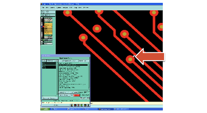
HDI Assembly Design for Manufacturability (DFM): Avoiding Costly Pitfalls
Even excellent materials and stack-ups can fail without strong HDI assembly design for manufacturability (DFM). DFM ensures the design is compatible with real-world fabrication, assembly, and inspection capabilities, directly improving yield, reliability, and cost efficiency.
Critical DFM considerations for HDI PCB assembly include:
- Microvia aspect ratio and plating reliability
- Minimum trace width/spacing and annular ring requirements
- Impedance control tolerances
- Thermal via placement and via-in-pad design
- Solder mask registration for fine-pitch pads
- Component placement clearances and stencil design
- Panelization and depanelization strategy for assembly
Early engagement with an experienced HDI manufacturer for DFM review is strongly recommended. Many costly revisions can be avoided by following conservative design rules and leveraging the fabricator’s process capabilities.
Our cluster page HDI assembly design for manufacturability DFM provides detailed rule sets, checklists, common pitfalls, IPC references, and practical layout strategies tailored specifically for microvia-intensive boards.
The HDI PCB Assembly Process and Best Practices
A typical HDI PCB assembly workflow includes DFM review, material procurement, sequential lamination and laser drilling, copper plating, fine-line imaging, surface finish application (ENIG is most common), SMT assembly with precise reflow profiling, X-ray inspection of BGA and microvia fills, AOI, ICT, functional testing, and reliability screening.
Key challenges in HDI assembly include warpage control, microvia plating quality, accurate registration across multiple laminations, solder joint reliability on small pads, and thermal management during reflow. Proven best practices — symmetric stack-ups, CTE-matched materials, conservative via structures, simulation-driven design, and rigorous process control — significantly improve outcomes.
Applications and Future Outlook
HDI PCB assembly is widely used in smartphones, AR/VR devices, medical wearables and implants, automotive ADAS, 5G/6G equipment, data center hardware, and aerospace avionics. Looking ahead, trends include finer features, embedded components, advanced low-loss and high-thermal materials, and tighter integration with semiconductor packaging.
Conclusion
HDI PCB assembly is a sophisticated discipline that demands excellence in material selection, stack-up design, and DFM. By deeply understanding HDI assembly stack-up structures and materials, selecting the right materials for HDI PCB assembly, and applying rigorous HDI assembly design for manufacturability DFM, you can achieve smaller, faster, more reliable electronic products with excellent manufacturing yields.
FAQs
Q1: What is the difference between 1+N+1 and 2+N+2 HDI stack-up structures?
A1: 1+N+1 is more cost-effective and suitable for moderate density, while 2+N+2 provides higher routing density and better electrical performance for complex high-speed designs. The choice depends on layer count, signal integrity, and thermal requirements. See our article on HDI assembly stack-up structures and materials.
Q2: How do I select the right materials for HDI PCB assembly?
A2: Focus on Dk, Df, Tg, CTE, and thermal conductivity that match your electrical, thermal, and reliability needs. Low-loss materials are preferred for high-speed designs; high-Tg and high-thermal-conductivity laminates suit power-dense applications. Detailed guidance is available in HDI assembly: selecting the right materials.
Q3: Why is DFM especially important in HDI PCB assembly?
A3: HDI designs have tighter tolerances for microvias, trace width, annular rings, and registration. Good DFM prevents plating voids, breakout, warpage, and assembly defects. Our guide to HDI assembly design for manufacturability DFM offers practical rules and checklists.
Q4: What surface finish is best for HDI PCB assembly?
A4: ENIG (Electroless Nickel Immersion Gold) is the most popular choice because it provides excellent solderability, flatness, and reliability for fine-pitch components and via-in-pad designs.


