










During routine CAM engineering review for a standard 4-layer FR-4 board specified with HDI features, our team encountered multiple interpretation challenges between the customer's design files and the production order parameters. What initially appeared as straightforward confirmations quickly evolved into a deeper investigation into via processing, soldermask alignment, and stackup verification. As Senior CAM Auditor, I led the review to ensure manufacturability without compromising the intended electrical performance.
The project involved a compact 63.5 x 127 mm single-panel PCB with 1oz inner and 2oz outer copper, 1.6mm finished thickness, ENIG surface finish, and laser blind vias. Production was set for 10 pieces with V-CUT depanelization. While the order parameters aligned with typical FR-4 capabilities, the Gerber and drill data presented subtle but critical conflicts that required clarification before releasing to lamination and drilling. This case highlights how even well-prepared files can harbor risks that only surface during detailed CAM analysis.
Understanding the Original Design Intent
The customer designed this 4-layer board ( #HDI-20260512-016 ) (HDI stage count: 1) for an electronics application requiring reliable signal integrity and compact layout. Key elements included 0.2mm minimum hole size, 6mil line width/space, green soldermask on both sides, and white silkscreen. The fabrication notes and order specified aluminum sheet plugging for vias and laser processing for blind holes. The stackup reference indicated a controlled build-up with blind vias to optimize layer transitions while maintaining overall thickness at 1.6mm ±10%.
From the design files, the intent was clear: leverage blind vias for density in critical areas while using standard through vias elsewhere, with via plugging to protect against contamination and ensure solderability. The SMT data suggested specific pad and mask openings optimized for assembly. Our initial data import showed the board was intended for 100% flying probe testing, with no impedance or other special requirements noted. This setup is common for modern compact modules, yet the transition from design software to manufacturing data often reveals gaps.
Our Engineering Findings During CAM Review
Upon loading the Gerber files, drill data, and fabrication notes into our CAM system, I immediately noticed discrepancies. The VIA layer contained through-hole and blind via definitions that did not perfectly align with the order's specified laser blind hole process and aluminum sheet plugging requirements. Additionally, the soldermask data conflicted with the SMT (paste) layer openings in several regions.
Our standard verification workflow flagged the need for confirmation on the attached stackup drawing for board thickness and copper weights (inner 1oz, outer 2oz). The silkscreen layer also required verification for adding only the factory production number without additional markings. Most critically, blind holes larger than 0.15mm in the original files needed adjustment to our laser drilling capability of 0.15mm.
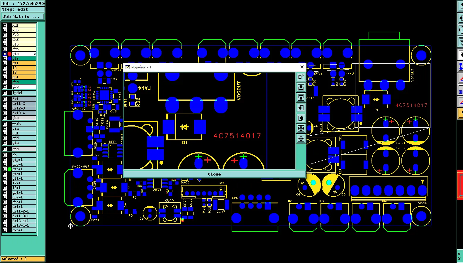
Figure 1: silkscreen layer adding only the factory production number
| Aspect | Customer Files | Order / Manufacturing Spec |
|---|---|---|
| Blind Vias | Various sizes >0.15mm | Laser drill 0.15mm |
| Via Plugging | VIA layer data | Aluminum sheet plug + oil per order |
| Soldermask vs SMT | Inconsistent openings | Soldermask data prioritized |
These findings prompted a formal Engineering Question (EQ) package to the customer for confirmation before proceeding with production files optimization.
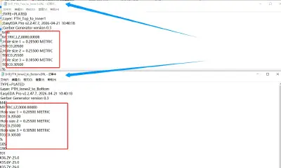
Figure 2: blind holes larger than 0.15mm files needed adjustment to our laser drilling capability of 0.15mm
Conflict Analysis
The dominant design-manufacturing conflict centered on via processing and data interpretation. The customer's original files defined blind vias with varying diameters exceeding our standard laser drill limit of 0.15mm for reliable HDI processing in this 4-layer configuration. According to IPC-6012 and common HDI guidelines, laser-drilled blind vias require precise diameter control to maintain aspect ratios and plating integrity. Adjusting larger vias to 0.15mm risked altering the intended electrical characteristics if not confirmed.
Compounding this was the via plugging specification. The order called for aluminum sheet plugging ("铝片塞孔"), yet the VIA layer data and fabrication notes suggested oil plugging compatibility. In our CAM review, we observed that mismatched plugging methods could lead to incomplete fill, potential voids during lamination, or solder wicking issues during assembly. This is a classic Data-to-Data and Design-to-Manufacturing conflict where Gerber definitions did not fully align with the stated process capabilities.
Simultaneously, soldermask data inconsistencies with SMT paste layers created ambiguity in pad exposure. Prioritizing soldermask per the original files was our default, but without confirmation, this could result in insufficient or excessive mask coverage, leading to solder bridge risks or poor wetting. The stackup verification was essential to ensure the final 1.6mm thickness and copper weights matched after lamination, as deviations here directly impact impedance and mechanical stability (per IPC-2221 considerations).
Without clarification, production could not proceed confidently. Potential risks included drill breakout on blind vias, incomplete plugging leading to reliability failures, or mask-related assembly defects. In my 15+ years of CAM auditing, such layered conflicts often stem from design tools not fully accounting for specific fab process windows.
Additional Findings That Supported the Investigation
Supporting observations included the need for single-panel (1x1) shipment verification with V-CUT and the precise silkscreen addition of only the factory number AIV-4C7514017. The SMT layer had been pre-optimized by the customer, but cross-checks with soldermask were still required. These elements reinforced the primary via and mask conflicts by highlighting the importance of full data-process alignment across all layers.
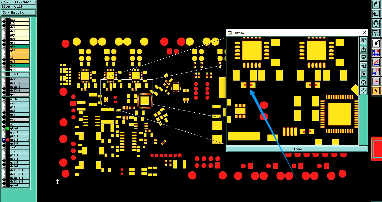
Figure 3: The solder mask data is inconsistent with the SMT data
Engineering Clarification and Final Resolution
We issued a detailed EQ package attaching the proposed production files, stackup drawing, and specific questions. The customer promptly confirmed:
- Soldermask data takes precedence; proceed as per original soldermask files.
- Stackup confirmed with 1.6mm ±10% thickness and inner 1oz / outer 2oz copper.
- Silkscreen limited to production number only.
- Blind holes adjusted to 0.15mm laser drill per our process.
- Via plugging per order (aluminum sheet compatible with oil where applicable).
- Production files and single-panel dimensions approved.
With these confirmations, we optimized the CAM data: adjusted drill files for laser compatibility, ensured proper plugging parameters, aligned mask openings, and generated final production artwork. The board was released for fabrication with 100% flying probe testing. This resolution prevented potential yield loss from misdrilled or poorly plugged vias and ensured the final panels met all mechanical and electrical expectations.
| Parameter | Original | Resolved |
|---|---|---|
| Blind Via Size | Variable >0.15mm | Standardized to 0.15mm laser |
| Via Plugging | Ambiguous | Aluminum sheet per order |
| Board Thickness | Specified 1.6mm | Confirmed ±10% |
Key Design Lessons for PCB Designers
- Clearly specify via types, sizes, and plugging methods in both fabrication notes and layer-specific files to avoid interpretation gaps.
- Ensure soldermask and SMT paste data are synchronized; provide explicit priority instructions if conflicts exist.
- Reference exact stackup drawings with tolerances for thickness and copper weights in the order details.
- For HDI boards, align blind via diameters with the fabricator's laser drilling capabilities early in the design phase.
- Limit silkscreen content to essentials and confirm any factory-specific markings in advance.
- Provide complete drill files with attributes distinguishing blind, buried, and through vias.
- Request pre-production file review for complex via or mask requirements to catch issues before full commitment.
- Document any design tool outputs that may deviate from standard manufacturing process windows.
FAQ
Q1: Why did differing blind via sizes in the design files trigger an Engineering Question?
A1: Larger vias required adjustment to our reliable 0.15mm laser drill process for HDI layers. Without confirmation, this could affect plating quality and signal integrity, per typical IPC-6012 standards for blind via reliability.
Q2: What risks arise when soldermask data conflicts with SMT layer data?
A2: Inconsistent openings can lead to solder bridges, insufficient coverage, or assembly defects. Prioritizing one dataset without confirmation risks yield loss during SMT.
Q3: How important is stackup confirmation during CAM review?
A3: Critical for ensuring final thickness, copper weights, and layer registration meet design intent after lamination. Mismatches can cause warpage or electrical failures.
Q4: Why specify via plugging methods explicitly?
A4: Different methods (e.g., aluminum sheet vs. resin) have varying impacts on reliability and downstream processes. Ambiguity can result in voids or contamination.
Q5: What should designers do when files and order specs conflict?
A5: Respond promptly to EQs with clear approvals. Early communication prevents production delays and ensures the final product matches the intended performance.
Q6: How does CAM review prevent manufacturing issues in HDI PCBs?
A6: By cross-verifying all data layers against process capabilities, identifying conflicts like via sizes or mask definitions before production starts.






