










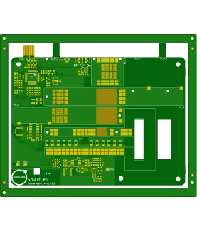
PCB Specifications
| Parameter | Value | Parameter | Value |
|---|---|---|---|
| PCB Type | HDI PCB | Quantity | 10 pcs |
| Layers | 4 Layers | Board Type | Panel PCB |
| Dimensions | 63.5 x 127 mm | Copper Weight | 2oz |
| Thickness | 1.6 mm | Min Track / Spacing | 6/6mil↑ |
| Surface Finish | ENIG (Immersion Gold) | Min Hole Size | 0.2mm |
| Solder Mask | Green | Silkscreen | White |
Manufacturing Timeline
Logistics Information
Key Manufacturing Processes
Manufacturing Summary
This 4-layer HDI board measured 63.5 × 127 mm with 1 oz inner and 2 oz outer copper and a 1.6 mm finished thickness using Shengyi S1000-2M TG170 material. Produced in a quantity of 10 pieces as single boards with V-cut separation, the design incorporated 6 mil line/space, blind vias standardized to 0.15 mm laser drilling, ENIG surface finish, and via tenting. The mixed copper weight and HDI stage 1 construction required precise stackup control for this small run.
DFM review confirmed the stackup for target board and copper thickness tolerances. Solder mask data was prioritized over paste layer discrepancies to ensure accurate opening sizes. Production numbering was added solely to the silkscreen layer as specified. Blind hole diameters from the original files were uniformly adjusted to 0.15 mm for laser drilling consistency. Via tenting followed the order requirements for plugged processing. SMT layer optimizations were applied and verified. These adjustments maintained design intent while addressing manufacturability limits for the mixed copper configuration.
All boards completed 100% flying probe testing successfully within the 17-day schedule. The final panels delivered consistent registration, plating, and surface quality suitable for assembly despite the blind via and copper weight considerations.
Explore More PCB Manufacturing Resources
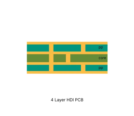
4 Layer HDI PCB Manufacturing Insights
These boards deliver high routing density through laser-drilled microvias and sequential lamination while maintaining controlled production costs.
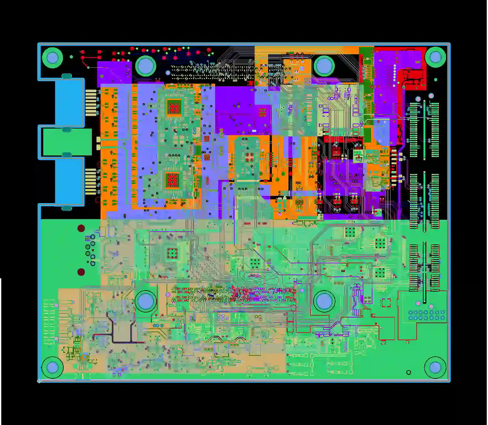
Multilayer HDI PCB Common Engineering Queries in Manufacturing
Senior PCB manufacturing engineer shares real factory insights on common engineering queries for multilayer HDI PCBs including 4 Layer HDI PCB, 6 Layer HDI PCB, 8 Layer HDI PCB, and 10 Layer HDI PCB. Learn about microvia stacking, registration challenges, impedance control, and practical DFM tips to reduce EQs and improve production yield.
Real Production Records
| Order ID | PCB Type | Layers | Dimensions | Solder Mask | Surface Finish | Quantity | Action |
|---|---|---|---|---|---|---|---|
| HDI-20260729-036 | HDI PCB | 8 | 97 x 93.4 | Black | ENIG (Immersion Gold) | 100 | View detail |
| HDI-20260720-0001 | HDI PCB | 8 | 188 x 100 | Matte Black | ENIG (Immersion Gold) | 125 | View detail |
| HDI-20260718-0002 | HDI PCB | 4 | 37 x 26.6 | Green | ENIG (Immersion Gold) | 20 | View detail |


