










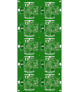
PCB Specifications
| Parameter | Value | Parameter | Value |
|---|---|---|---|
| PCB Type | HDI PCB | Quantity | 10 pcs |
| Layers | 4 Layers | Board Type | Panel PCB |
| Dimensions | 210 x 100 mm | Copper Weight | 1oz |
| Thickness | 1 mm | Min Track / Spacing | 4/4mil |
| Surface Finish | OSP | Min Hole Size | 0.1mm |
| Solder Mask | Green | Silkscreen | White |
Manufacturing Timeline
Logistics Information
Key Manufacturing Processes
Manufacturing Summary
This order consisted of 10 panels of a 4-layer HDI PCB, each measuring 210 x 100 mm with 1.0 mm thickness and 1 oz copper weight. Featuring 4/4 mil trace and spacing, 0.1 mm minimum hole size, blind vias, and a custom stackup, the boards required precise process control during fabrication. OSP surface finish was selected, paired with green soldermask and white silkscreen lettering.
Manufacturing commenced with engineering review and material preparation, followed by inner layer imaging, circuit etching, and careful layer stack alignment prior to high pressure lamination. The blind vias demanded accurate drilling and plating sequences. Solder mask application, organic coating for the OSP finish, anti-oxidation treatment, and comprehensive electrical testing completed the workflow.
The production was executed over 7.8 days, yielding panels with consistent layer registration and reliable via integrity. This approach ensured the tight-geometry multilayer boards met all specified requirements for the customer.
Explore More PCB Manufacturing Resources
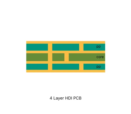
4 Layer HDI PCB Manufacturing Insights
These boards deliver high routing density through laser-drilled microvias and sequential lamination while maintaining controlled production costs.
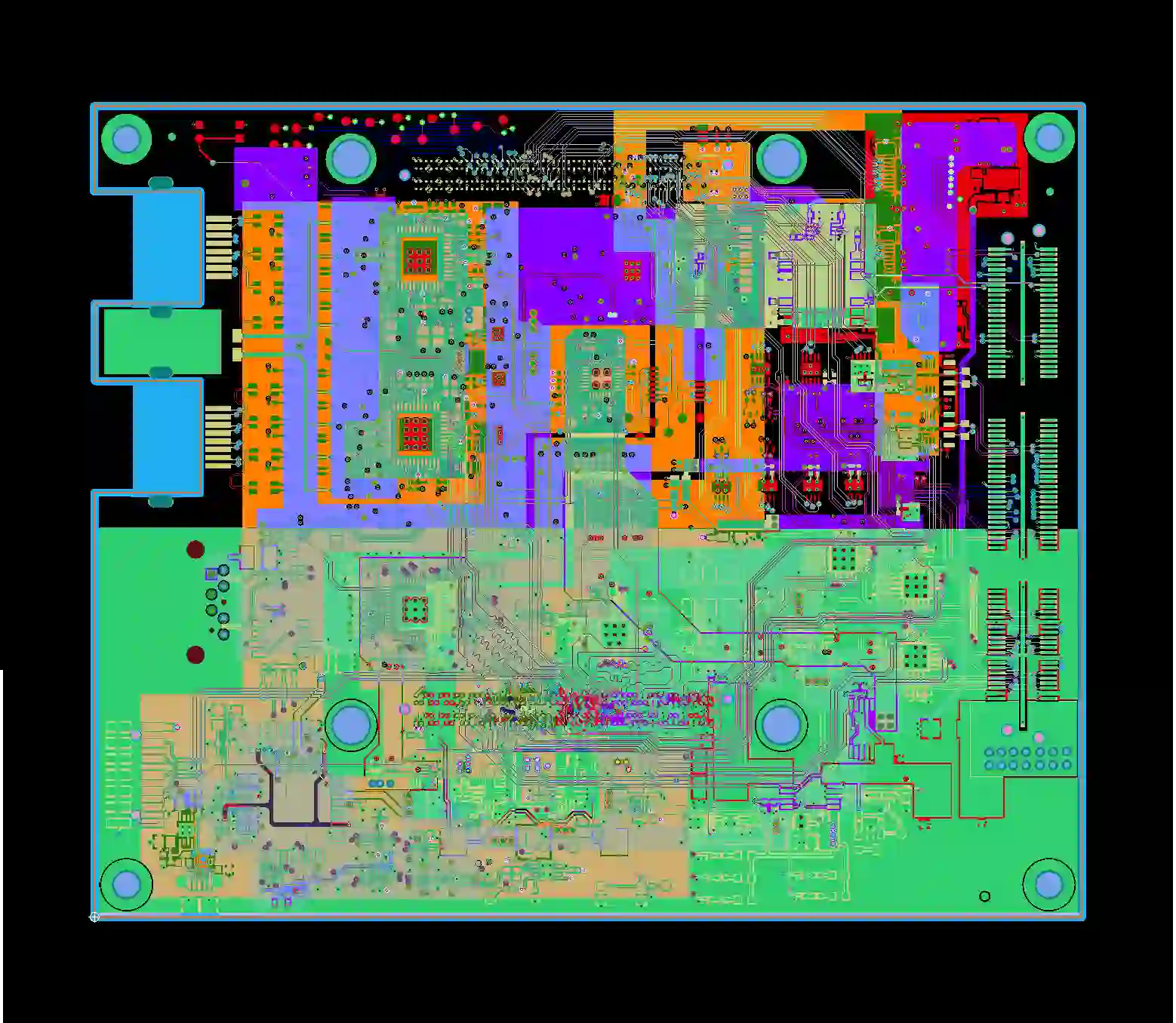
Multilayer HDI PCB Common Engineering Queries in Manufacturing
Senior PCB manufacturing engineer shares real factory insights on common engineering queries for multilayer HDI PCBs including 4 Layer HDI PCB, 6 Layer HDI PCB, 8 Layer HDI PCB, and 10 Layer HDI PCB. Learn about microvia stacking, registration challenges, impedance control, and practical DFM tips to reduce EQs and improve production yield.
Real Production Records
| Order ID | PCB Type | Layers | Dimensions | Solder Mask | Surface Finish | Quantity | Action |
|---|---|---|---|---|---|---|---|
| HDI-20260718-0002 | HDI PCB | 4 | 37 x 26.6 | Green | ENIG (Immersion Gold) | 20 | View detail |
| HDI-20260512-016 | HDI PCB | 4 | 63.5 x 127 | Green | ENIG (Immersion Gold) | 10 | View detail |
| HDI-20260422-051 | HDI PCB | 4 | 210 x 100 | Green | OSP | 10 | View detail |


