In our CAM engineering review for a recent 16-layer HDI order, several critical manufacturability issues emerged that required detailed clarification with the customer. This case highlights the common tension between aggressive design targets and the practical constraints of multilayer PCB fabrication, particularly when balancing board thickness, copper weights, and high-density features like blind vias and overlapping structures.
Our team identified risks in stackup configuration, via treatment, panelization method, and solder mask definition. These issues, if left unaddressed, could lead to delamination, poor plating, soldering defects, or assembly failures. As a senior CAM engineer with over 15 years in PCB fabrication, I always emphasize that early EQ communication prevents costly production delays and scrap.
Order Overview
This project involved a 16-layer FR-4 HDI board ( #FR4-20260326-008 ) with TG170 material, targeting a finished thickness of 2.2mm. The outer copper weight was specified at 2oz with inner layers at 1oz, using ENIG surface finish. Minimum hole size was 0.1mm, with line width/space at 4 mil, making it a high-density design requiring careful impedance and registration control. Blind vias were present (HDI count: 2), and the board size was compact at approximately 20.2 × 32.3mm. Quantity was 375 pieces (25 sets), with 100% flying probe testing required.
Panelization was set to 3×5 with 4mm process edges on all sides. The design called for resin plugging of vias, mechanical forming, and stamp hole connections. Production notes indicated the need for electrical testing reports and quality certificates. While the specifications looked straightforward on paper, the combination of thin dielectrics, thick copper, and dense via structures triggered multiple engineering flags during our DFM review.
Main Engineering Questions Found During CAM Review
Stackup and Copper Thickness Conflicts
The most significant issue was the mismatch between the requested 2.2mm finished board thickness and the provided stackup data. Our engineer noticed that the customer's dielectric thicknesses were extremely thin, especially when pairing with 2oz copper layers. After initial calculations, we determined that using the factory's thinnest 2oz core (0.11mm without copper) would push the final thickness closer to 2.65mm ±10%, risking delamination during lamination due to insufficient resin flow and pressure distribution.
Figure 1: customer's dielectric thicknesses were extremely thin
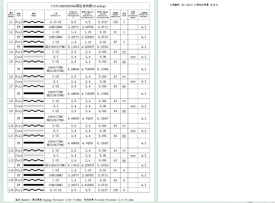
Figure 2: PCB stackp adjusted by our engineer
Additionally, the small 4 mil line width/space on outer layers made 2oz copper problematic. We observed that heavy copper would require excessive etching compensation, potentially breaking narrow copper bridges and causing open circuits or inconsistent impedance. Our CAM team recommended prioritizing the 2.2mm thickness target by adjusting outer layers (1,2,3,14,15,16) to 1oz copper while keeping internal layers at 2oz where possible. This compromise maintained signal integrity in critical areas while ensuring manufacturable dielectric spacing.
If ignored, the thin dielectrics could lead to resin voids, layer-to-layer separation under thermal stress, or severe board warpage after pressing. In extreme cases, this results in scrap boards during electrical testing or assembly reflow. We have seen similar high-layer count boards fail IPC-6012 Class 2 reliability tests due to such stackup deviations.
Via Overlap with SMD Pads and Resin Plugging Requirement
Multiple through-hole vias overlapped with SMD pads in the Gerber data. Without proper treatment, this would cause pad lifting or missing copper during drilling and plating, directly impacting soldering reliability. We strongly suggested resin plugging as per the fabrication notes to ensure flat, reliable pads.
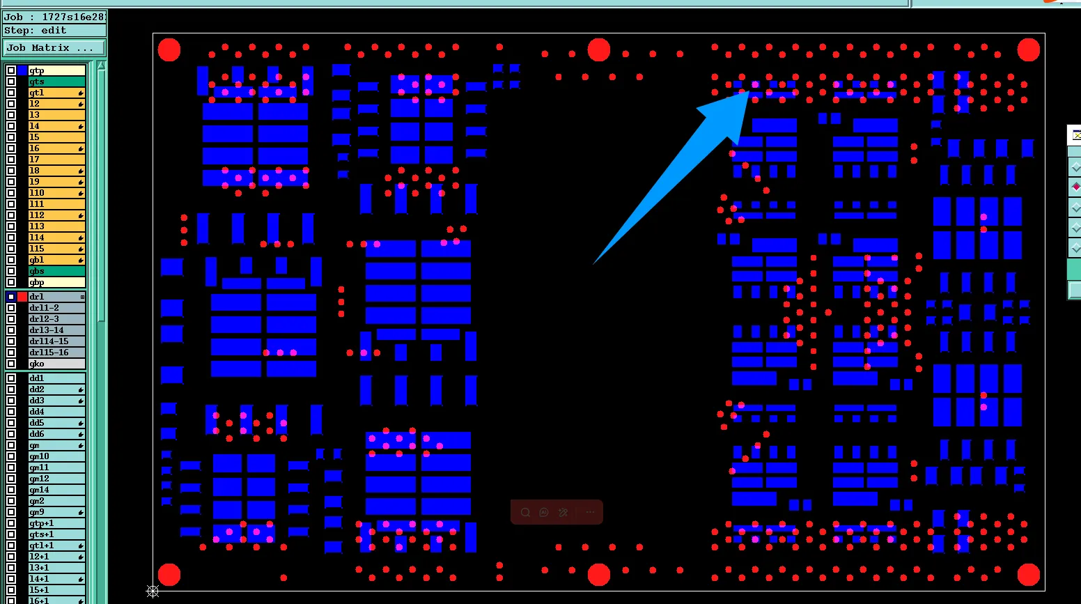
Figure 3: through-hole vias overlapped with SMD pads
Our engineer confirmed that for blind vias and controlled-depth holes (six specific holes indicated in the design), bottom-side solder mask windows needed removal after depth control processing to avoid unnecessary exposure. The large no-copper hole openings in the solder mask data were also oversized, which could expose underlying copper and create short risks. We adjusted these windows to be only 0.1mm larger per side than the hole.
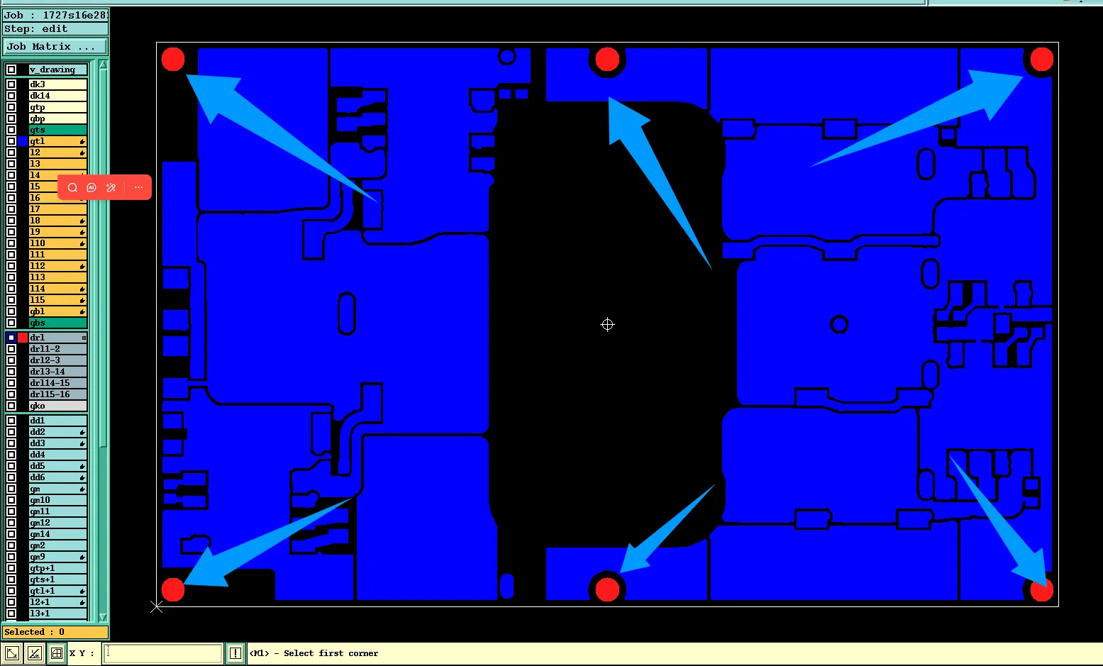
Figure 4: bottom-side solder mask windows of blind vias and controlled-depth holes needed removal

Figure 5: no-copper hole openings were also oversized
Had we proceeded without clarification, solder mask misalignment or incomplete plugging could cause poor solderability, via cracking during thermal cycling, or assembly failures. Resin voids in plugged vias are a common cause of field returns in HDI boards under vibration or temperature extremes.
Panelization and Process Edge Considerations
Given the compact board size and 4mm process edges, standard routing or V-cut was not feasible without compromising panel strength. Our team determined that stamp hole connections were the only viable option for the 3×5 array. This method provides better support during handling but requires precise fiducial placement and careful depanelization to avoid edge damage.
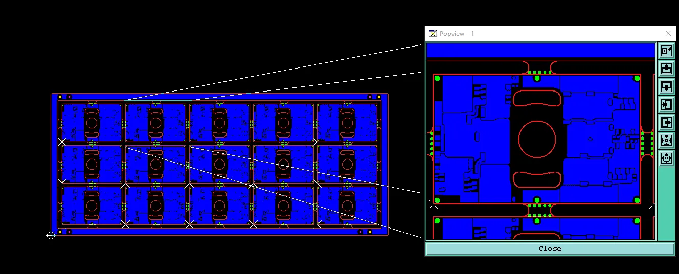
Figure 6: stamp hole connections
We also flagged the need to add version numbering on the solder mask layer since no silkscreen characters were present in the data, as requested in the order notes. These adjustments align with standard DFM practices for efficient panel utilization and traceability.
Manufacturing Risks and DFM Insights
This case underscores several recurring customer design challenges in high-layer HDI boards. Overly aggressive dielectric thinning to hit exact thickness targets often conflicts with resin flow requirements during high-pressure lamination, especially with mixed copper weights. Small trace geometries combined with thick copper exacerbate etching undercut, increasing the risk of necking or open circuits.
Via-to-pad overlaps without explicit plugging instructions frequently lead to production halts. Ignoring these can cause immediate assembly defects or long-term reliability failures under thermal stress. Panelization choices based solely on board outline without considering process edge width commonly force last-minute changes, delaying tape-out.
From our factory perspective, these issues typically trigger 2-3 review cycles, increasing engineering time and potential cost. Following IPC-2221 guidelines for minimum spacing and IPC-A-600 for acceptability helps, but real-world CAM data review is essential to catch stack-specific problems.
How the Engineering Team Resolved the Issues
Our team proposed a revised stackup with adjusted dielectric thicknesses to achieve the target 2.2mm ±10% while maintaining structural integrity. Copper weights were optimized per layer group to balance etchability and current-carrying needs. We confirmed resin plugging for all overlapping vias and implemented controlled-depth drilling for the specified holes, removing unnecessary bottom solder mask openings.
For panelization, we switched to stamp hole connections and verified fiducial protection. Solder mask windows were tightened, and version numbering was added to the solder mask layer. After customer confirmation on all points, the production data was updated and re-verified. We also adjusted the lamination parameters slightly to accommodate the final stackup.
Throughout the process, clear communication ensured the customer's design intent was preserved as much as possible while fitting within manufacturing capabilities.
Final Manufacturing Outcome
All EQ items were clarified and resolved. The stackup was finalized with the adjusted copper distribution and dielectric thicknesses. Panelization, via plugging, and solder mask modifications were implemented. The job received full CAM approval and was released for production with the optimized parameters. The boards are scheduled to meet the 35-day delivery window using standard FR-4 TG170 material and ENIG finish.
Key Takeaways for PCB Designers
- Provide detailed stackup drawings with exact dielectric thicknesses and copper weights early. Allow reasonable tolerance (±10% thickness) to accommodate real lamination results.
- Clearly specify via plugging requirements when vias overlap surface pads. Indicate controlled-depth holes in fabrication notes with layer references.
- Verify panelization feasibility against board size and process edge width before final Gerber output. Stamp holes are often necessary for small dense panels.
- Ensure solder mask data matches drilling and plating intent. Oversized openings near holes can expose copper unintentionally.
- Include version marking instructions if no silkscreen layer is used. Consistent fabrication notes reduce ambiguity.
- Balance copper thickness with minimum trace width/space. Heavy copper on fine features often requires engineering adjustments.
- Perform preliminary DFM checks for HDI designs with blind vias, focusing on registration and annular ring requirements per IPC-6012.
- Share complete ODB++ or Gerber + drill files with layer stack notes to speed up CAM review.
FAQ
Q1: Why is resin plugging critical when vias overlap SMD pads?
A1: Without plugging, drilling and plating can damage or lift the pad copper, leading to missing pads or unreliable solder joints. Resin ensures a flat, solid surface for component attachment and prevents voids that could cause failures during reflow or in the field.
Q2: What causes delamination risk in thin-dielectric multilayer stacks?
A2: Insufficient resin volume and high pressure requirements with thin cores lead to poor bonding. Combined with thick copper, this creates stress concentrations. Factories often adjust dielectrics or copper weights to maintain reliable lamination per IPC-TM-650 standards.
Q3: Why choose stamp hole panelization for small boards?
A3: For compact panels with wide process edges relative to board size, V-cut or tab routing may weaken the panel or damage boards during depanelization. Stamp holes provide better mechanical support while allowing clean separation.
Q4: How do CAM engineers handle copper thickness conflicts with fine features?
A4: We evaluate etching compensation needs and may reduce outer layer copper weight to prevent trace necking or opens. This decision balances current capacity, impedance, and manufacturability based on actual production data.
Q5: What risks arise from oversized solder mask openings around holes?
A5: Excessive openings can expose copper traces or pads near holes, leading to shorts, oxidation, or cosmetic defects. Tightening to 0.1mm per side ensures proper coverage while maintaining clearance for plating.
Q6: Why do factories adjust stackups during review?
A6: Customer-provided data often uses ideal thicknesses that don't match available core and prepreg materials. Adjustments ensure the final board meets thickness, impedance, and reliability requirements without delamination or warpage risks.