In the CAM review for this 2-layer 310×310mm FR-4 board, several manufacturability concerns surfaced related to board outline proximity, hole pad definitions, and fabrication data consistency. Large panels with V-cut plus routing demand extra attention to edge clearance and mechanical forming to avoid post-routing defects.
As a senior CAM engineer, I reviewed the files and raised targeted EQs to protect yield. Issues like traces too close to the outline and vias with inconsistent solder mask windows are classic triggers that, if ignored, can cause exposed copper, burrs, or assembly problems. Early clarification is essential for quick-turn jobs like this 2-day order.
Order Overview
This 2-layer FR-4 board ( #FR4-20260204-067 ) features 1oz copper on both sides, 1.0mm finished thickness, and TG150 material. It uses lead-free HASL surface finish with green solder mask and white silkscreen. Minimum hole size is 0.3mm and line width/space is 5 mil. The panel consists of two boards with customer self-panelization, V-cut combined with routing segmentation, and zero process edge. Quantity is 50 pieces (50 sets). 100% flying probe testing was specified, along with electrical test reports and quality certificates.
The large board size combined with tight edge clearances and mixed mechanical processes made this case particularly sensitive to DFM details.
Main Engineering Questions Found During CAM Review
Copper to Outline Clearance Issues
During the CAM review, we identified multiple locations where copper traces and pads were positioned too close to the board outline. For this panel using combined V-cut and routing segmentation, our standard DFM rules require a minimum 0.2mm clearance from routing edges and 0.35mm from V-cut lines.
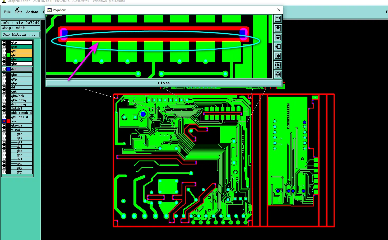
Figure 1, 2: copper traces and pads were positioned too close to the board outline
We noticed several violations that posed significant risks. Our engineer highlighted this immediately because insufficient clearance often leads to exposed copper, burrs, or copper peeling after mechanical depanelization. If the EQ had been ignored and production continued as-is, the boards would likely suffer from cosmetic defects, edge short circuits, or lifted copper during assembly and handling, resulting in higher scrap rates and potential field failures.
To mitigate this, we asked the customer to confirm acceptance of the current design or approve necessary adjustments. This type of issue is one of the most common triggers for EQs on large 2-layer panels with tight mechanical processes.
Asymmetric Hole Pad Definitions
Another key concern involved through-hole attributes. The customer data showed asymmetric pad configurations on specific holes: the 2.6mm hole and several 0.4mm holes (clearly marked by arrows) had copper pads on one side only, with no corresponding pads on the opposite side.
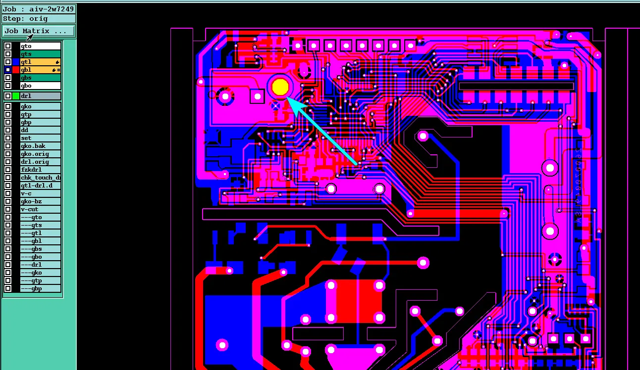
Figure 3: the hole had copper pads on one side only
This configuration is unusual for standard 2-layer through-hole boards and directly impacts drilling programs, plating parameters, and annular ring reliability. Without confirmation, we could not safely determine whether this was intentional (e.g., for specific component mounting) or a design oversight. Proceeding without clarification risked weak plating, hole breakout, or unreliable electrical connectivity under thermal or mechanical stress.
Our team requested explicit confirmation of the hole attributes to ensure correct manufacturing parameters were applied, aligning with IPC-6012 standards for through-hole reliability.
Solder Mask, Silkscreen Layer, and Panel Features
Several secondary but important issues were also identified. Silkscreen characters were placed on the GKO (outline) layer rather than the proper GTO top silkscreen layer. Additionally, the fabrication notes specified via cover oil (tenting), yet multiple arrowed vias showed double-sided solder mask openings.
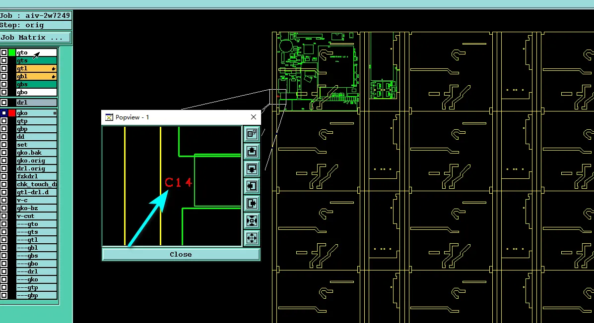
Figure 4: silkscreen characters were placed on the GKO (outline) layer
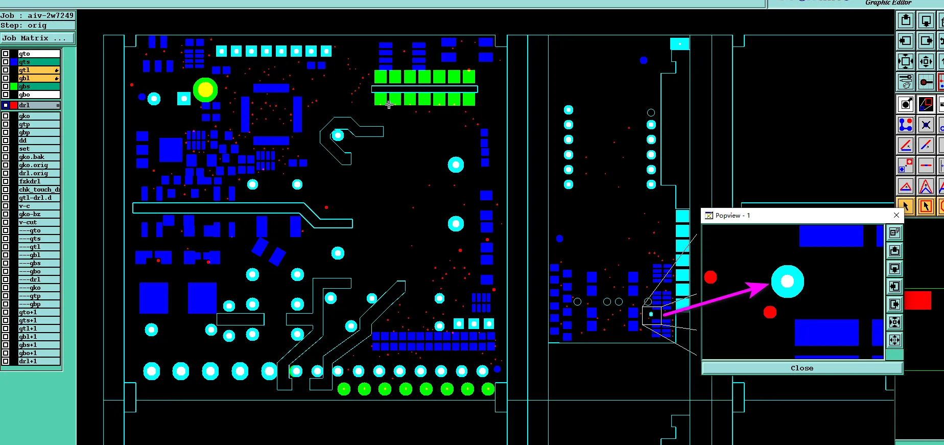
Figure 5: multiple arrowed vias showed double-sided solder mask openings
We further noted the absence of standard locating holes and fiducial marks on the panel edges, along with etch text designed at only 1mil width (well below reliable manufacturability limits). We proposed standard solutions: relocating the markings, adjusting via windows for consistency, enlarging the text to 6mil minimum, and adding conventional fiducials and locating holes.
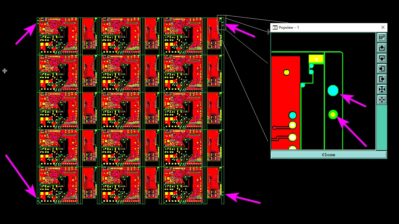
Figure 6: absence of standard locating holes and fiducial marks
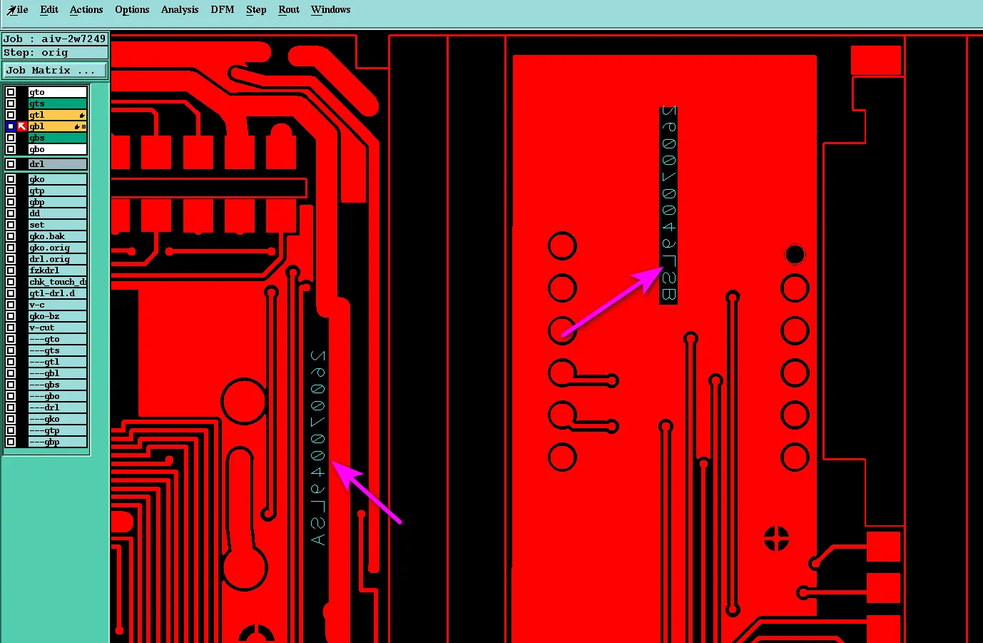
Figure 7: etch text designed at only 1mil width
These details, while seemingly minor, can cause missing or misplaced markings, registration errors during production, unreadable text, and solder-related defects during assembly. Confirming them helped us align the production files accurately with both customer intent and factory capabilities.
Manufacturing Risks and DFM Insights
Large 2-layer panels with mixed V-cut and routing are prone to edge-related defects when copper features approach the outline. Asymmetric pads often indicate design intent that needs explicit confirmation to avoid plating inconsistencies. Small text and misplaced layers are frequent oversights that extend review time.
These issues commonly cause production delays, extra engineering cycles, or yield loss from burrs and exposed copper. In our experience, insufficient edge clearance is one of the top reasons for cosmetic and functional failures after mechanical forming.
How the Engineering Team Resolved the Issues
We received customer confirmation on all points. Hole attributes were clarified, characters moved to the correct silkscreen layer, and via solder mask windows adjusted per the cover oil requirement. Edge clearance risks were acknowledged, with the design accepted as-is or with minor factory compensation. Standard fiducials and locating holes were added to the panel, and text was enlarged for manufacturability.
Our CAM adjustments ensured the files were production-ready while staying faithful to the original design intent.
Final Manufacturing Outcome
All EQs were resolved through confirmation and targeted file updates. The panel data, clearances, and layer definitions are now aligned. The order has been approved and released for production on the 2-day schedule.
Key Takeaways for PCB Designers
- Maintain adequate copper-to-outline clearance (≥0.2mm for routing, ≥0.35mm for V-cut) to prevent edge defects.
- Clearly define hole attributes when pads are asymmetric or missing on one side.
- Place all silkscreen elements on the correct layer (GTO/GBO) rather than outline layers.
- Ensure solder mask data matches fabrication notes for via tenting or plugging.
- Include fiducials and locating holes on panel edges for accurate processing.
- Design text and features above minimum manufacturable sizes (typically 6mil for etch).
- Provide complete fabrication notes that align with actual Gerber data.
- Review files for V-cut + routing compatibility on large panels.
FAQ
Q1: Why is copper-to-edge clearance critical in V-cut + routing panels?
A1: Insufficient clearance often causes exposed copper, burrs, or peeling after depanelization, leading to cosmetic defects or short circuits. Proper spacing protects traces during mechanical forming.
Q2: What does asymmetric pad configuration mean for through holes?
A2: It indicates pads on one side only. Confirmation is needed to set correct drilling and plating parameters, preventing weak connections or reliability issues.
Q3: Should silkscreen text be placed on outline (GKO) layers?
A3: No. Text belongs on dedicated silkscreen layers (GTO/GBO). Placement on outline layers can result in missing or misplaced markings.
Q4: Why add fiducials and locating holes to customer panels?
A4: They ensure accurate alignment during drilling, imaging, and routing. Missing marks can cause registration errors on large panels.
Q5: What happens if etch text is designed below minimum size?
A5: Fine text (e.g. 1mil) becomes unreadable or disappears during etching. Factories enlarge to reliable minimums (around 6mil) for clear legibility.