During CAM review of a recent 2-layer FR-4 order, our team focused on data consistency, customer-specific marking requirements, and milling outline preparation. Although this was a standard 2-layer board, several clarification points arose regarding fabrication files, silkscreen content, and process data alignment. These issues are typical in quick-turn jobs where clear communication prevents production errors.
As a senior CAM engineer, I always stress that even simple boards benefit from thorough DFM checks. In this case, we confirmed silkscreen additions, verified milling data, and addressed missing layers to ensure smooth fabrication and assembly. Ignoring such details can lead to incorrect markings, incomplete solder paste data, or dimensional inaccuracies after routing.
Order Overview
This 2-layer FR-4 board ( #FR4-20260209-088 ) used TG150 material with 1oz copper on both sides and a finished thickness of 1.6mm. Surface finish was ENIG, with green solder mask and white silkscreen. Minimum hole size was 0.3mm and line width/space 6 mil. Board dimensions were 144 × 208mm, panelized 2×3 with customer self-panelization and V-cut segmentation. Quantity was 30 pieces (5 sets). The job required 100% flying probe testing and included customer notes for milling by MILLING.gbr. Production was confirmed with a short 2-day turnaround.
While straightforward in layer count, the combination of custom silkscreen requirements and specific milling data necessitated careful file cross-checking before proceeding to production.
Main Engineering Questions Found During CAM Review
Silkscreen Marking and Logo Requirements
The customer requested specific markings on the top layer, including our factory UL logo, anniversary notation, and related identifiers. We noticed slight variations in the description across communications. Our CAM team confirmed the exact content to be added to the top silkscreen layer to avoid any mismatch with customer expectations.
Figure 1: customer requested specific markings on the top layer
We also updated an arrow-indicated area with the latest factory numbering as per the new file submission. These markings ensure traceability and compliance. If the markings had been applied incorrectly, it could result in boards with wrong version identifiers or missing certification logos, leading to quality audit failures or customer rejection during incoming inspection.
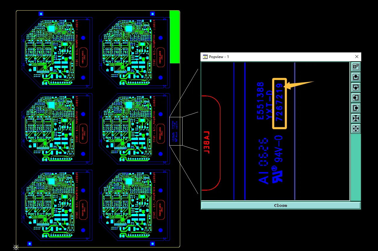
Figure 2: latest factory numbering as per the new file submission
Milling Data and Outline Processing
The customer note explicitly stated "milling by MILLING.gbr". We verified that the provided milling layer aligned with the board outline and V-cut requirements. With zero process edge specified and customer self-panelization, precise milling data is critical for mechanical forming accuracy.
Our engineer paid special attention to this because any misalignment between the milling file and the overall panel data could cause dimensional deviations or rough edges after routing. In past cases, mismatched outline data has led to scrap during depanelization or assembly fixture incompatibility.
Missing Solder Paste Layer and File Confirmations
The submitted files lacked a solder paste layer. We raised this for confirmation, as paste data is essential for accurate stencil creation in SMT assembly. Multiple file confirmation points were also clarified, including the new transmitted files and arrowed updates.
Proceeding without paste data clarification could result in incomplete stencil files, causing poor solder paste deposition, tombstoning, or insufficient joints during assembly. We always prefer explicit confirmation on such details to protect both manufacturing yield and downstream assembly success.
Manufacturing Risks and DFM Insights
Even on simple 2-layer boards, discrepancies in fabrication notes versus actual Gerber data frequently trigger EQs. Custom silkscreen requirements are a common source of misalignment if not explicitly confirmed. Missing layers like solder paste often go unnoticed by designers but directly impact assembly readiness.
Milling data that doesn't perfectly match panelization intent can cause tolerance stack-up issues during mechanical routing. These small oversights can delay quick-turn jobs, increase engineering back-and-forth, or lead to boards that fail customer incoming QC due to incorrect markings or dimensional errors.
According to IPC-A-600 acceptability criteria, clear identification and accurate outline processing are key to reliable delivery. Our review process catches these before they become costly problems downstream.
How the Engineering Team Resolved the Issues
We confirmed the exact silkscreen content with the customer, applying the UL logo, anniversary marking, and latest factory numbering as indicated. The milling layer was verified against the board outline, and we received confirmation to proceed despite the missing paste layer (with a note for future submissions). All file updates were cross-checked and approved.
Our team made minor adjustments to ensure marking placement did not interfere with copper features or solder mask openings. This DFM optimization maintained full compliance with the customer's requirements while fitting standard production workflows.
Final Manufacturing Outcome
All engineering questions were resolved through customer confirmations. Files were updated with correct silkscreen markings and milling data verified. The job was approved for production with the clarified parameters and is proceeding on the 2-day schedule.
Key Takeaways for PCB Designers
- Always include a complete set of Gerber files, including solder paste layers, even for prototype runs.
- Clearly specify custom silkscreen requirements (logos, UL marks, version numbers) in fabrication notes with layer references.
- Provide dedicated milling or outline layers when using non-standard routing. Ensure they align with panelization intent.
- Cross-check panelization method (self-panel vs factory) and process edge settings early in the design phase.
- Use consistent naming and arrow indicators in design files when requesting specific modifications.
- Submit updated files promptly when version changes occur to avoid numbering conflicts.
- Document any special markings or certifications needed for traceability and compliance.
- Perform a final Gerber review for layer completeness before upload to reduce EQ cycles.
FAQ
Q1: Why is it important to confirm custom silkscreen markings like UL logos?
A1: Incorrect or missing certification markings can cause compliance issues or customer rejection. CAM review ensures the added content matches requirements without overlapping functional areas.
Q2: What problems can arise from a missing solder paste layer?
A2: Without paste data, stencil creation becomes inaccurate, leading to insufficient or excessive solder paste, which causes assembly defects like open joints or bridging.
Q3: Why verify milling data separately in PCB fabrication?
A3: Milling files define the final board contour and slots. Mismatches with panel data can result in incorrect dimensions, rough edges, or damage during depanelization.
Q4: How do factories handle version updates indicated by arrows in design files?
A4: We update the specified areas with current factory numbering or revisions and seek confirmation to ensure the change aligns with customer intent before etching.
Q5: Is file confirmation necessary even for simple 2-layer boards?
A5: Yes. Quick-turn jobs with custom requirements still need verification of layers, markings, and outline data to prevent avoidable errors and ensure first-pass success.