We received a long single-layer FPC, 18.5 mm by 190 mm, built on 0.1 mm rolled copper. The data package called for a 0.1 mm PI stiffener in two places and, at the same time, listed a finished total thickness of 0.30 mm in those stiffened zones. That combination stopped us right away. A 0.1 mm base plus a 0.1 mm PI simply does not add up to 0.30 mm. The rest of the stack—1 oz / ½ oz copper, laser outline, hard gold at 1 µin over 120 µin nickel—was straightforward. The thickness call-out was not.
This was a small run, only 25 pieces (5 sets), but the process still had to be right. We needed to know whether the requested FPC stiffener thickness could actually be built, and if not, what controlled alternative would still give the customer a functional part. The review focused on the physical limits of the materials and on keeping every step inside a stable manufacturing window.
Why 0.1 mm PI Plus 0.1 mm Base Cannot Reach 0.30 mm
The oder ( #FPC-20260413-058 ) fabrication notes listed base thickness 0.1 mm and PI stiffener 0.1 mm. They also asked for 0.3 mm overall thickness in the stiffened areas. When we looked at the actual materials, the math was simple. A typical 0.1 mm rolled-copper FPC already includes its own polyimide core and copper. Adding a 0.1 mm PI stiffener with a normal adhesive layer lands you somewhere around 0.18–0.22 mm after press and cure. There is no realistic way to stretch that stack to 0.30 mm without changing the stiffener thickness itself.
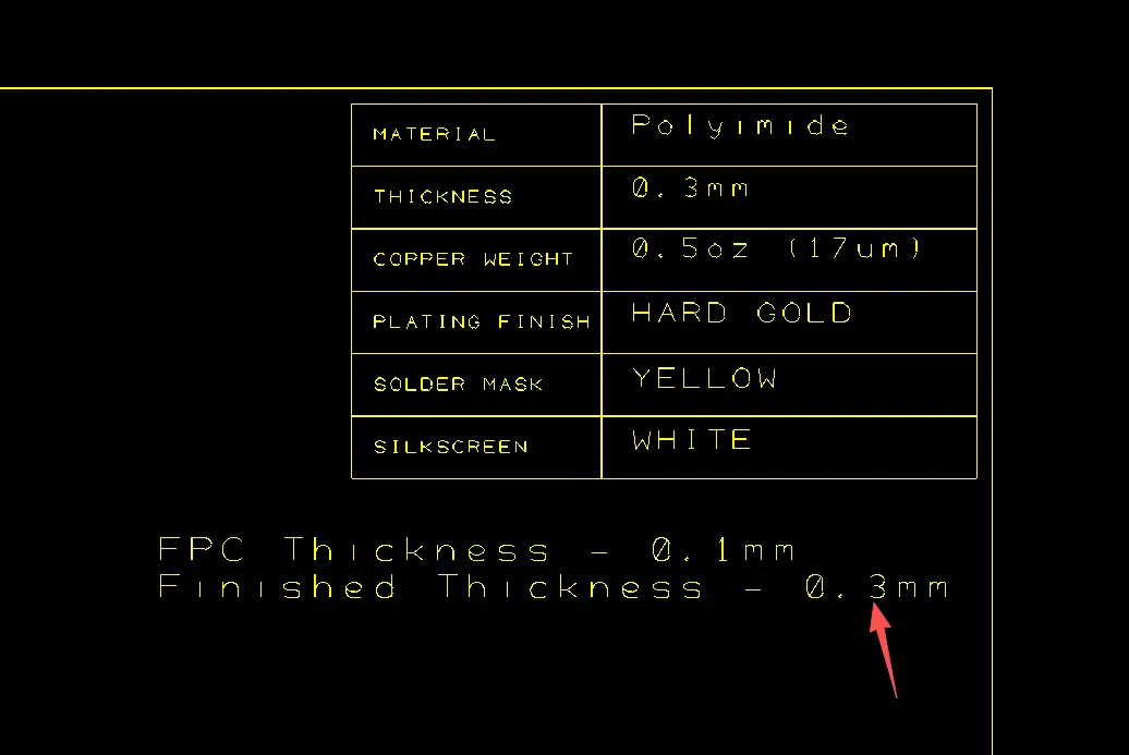
Figure 1: The Gerber design requires a finished thickness at 0.3mm
We flagged it as an Engineering Question. Leaving the 0.1 mm PI in place would have produced a part that was roughly 0.10 mm thinner than the drawing called for. In a gold-finger or connector application that undersize can mean weak contact pressure or a mechanical fit problem later. Production could not start until the thickness requirement was clarified or the construction was adjusted.
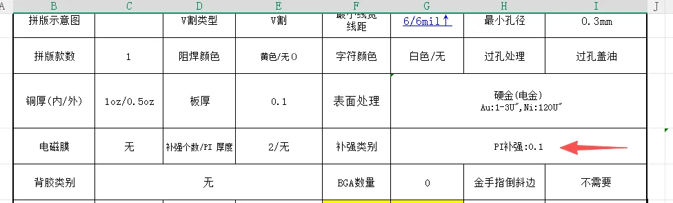
Figure 2: 0.1 PI stiffener
Zone-Specific Thickness Windows for Finger and Connector Ends
Rather than push the original stack, we suggested a practical control plan that still met the functional need at each end of the strip:
- Finger end (hard-gold contact area): FPC + PI total thickness 0.30 ± 0.03 mm
- Connector end: FPC + PI total thickness 0.30 ± 0.05 mm
The tighter window at the finger end protects contact reliability. The slightly looser window at the connector end gives the process more breathing room without hurting function. Both numbers stay inside what we can hold once the right PI film and adhesive are chosen.
| Zone | Original Request | What We Proposed | Why It Works |
|---|---|---|---|
| Finger (gold contact) | 0.30 mm | 0.30 ± 0.03 mm | Tighter control for reliable mating |
| Connector end | 0.30 mm | 0.30 ± 0.05 mm | Wider window, still functional |
| Open flex area | 0.10 mm base | 0.10 ± 0.02 mm | Normal rolled-copper range |
How Base, PI Film, and Adhesive Variation Set the Real Thickness Window
Three things set the finished thickness of an FPC with stiffener: the base laminate, the PI film, and the adhesive after cure. Each one carries its own variation. A 0.1 mm rolled-copper base typically runs ±0.015 mm to ±0.020 mm. A 0.1 mm PI film adds another ±0.010 mm to ±0.015 mm. The adhesive layer, even when carefully controlled, usually contributes another ±0.010 mm once it has flowed and cured.
Stack those numbers and you end up with a finished thickness centered near 0.20 mm and a realistic process window of about ±0.03 mm under good control. Hitting a 0.30 mm centerline with the same materials is outside that window. IPC-6013 dimensional guidance for flexible boards treats thickness call-outs that exceed the sum of the listed materials as items that need clarification before tooling. That is exactly the situation we faced.
Laser forming makes the problem more visible. The laser focus and power are set for the local thickness. If the stiffened area is thinner than the drawing expects, or if the step between flex and stiffener is larger than planned, you can get rough edges, incomplete cuts, or local burning. Keeping the actual thickness both known and stable is the only way to keep the laser parameters consistent along a 190 mm strip.
Adhesive Flow Control and the Need for Thicker PI Film
FPC Stiffener attachment is done by hot-bar or vacuum press. The adhesive has to wet the surface properly without squeezing out past the edge of the PI. Too much flow drops the local thickness. Too little flow leaves voids that show up later as thickness scatter or delamination risk when the part is flexed. To reach a true 0.30 mm total we would normally pick a thicker PI film—something in the 0.18–0.20 mm range—plus an adhesive system whose cured thickness lands us on target. A 0.1 mm film simply cannot close the gap.
If we had built the part with the original 0.1 mm PI, the finished thickness would have sat about 0.10 mm below the documented requirement. That is a real mechanical risk for any connector or gold-finger interface designed around 0.30 mm.
Temporary Lead Wire for Isolated Hard-Gold Pads
The FPC surface finish was electrolytic hard gold, 1 µin gold over 120 µin nickel. Two pads in the design were completely isolated. Electrolytic plating needs a continuous current path. Without one, those pads get little or no gold.
We recommended plating one of the isolated pads normally and adding a single temporary lead wire to the second pad so it could share the plating bus. After plating the lead is cut away. This is standard practice and keeps gold thickness uniform. Once the customer agreed to the lead wire, the plating step returned to a normal, high-yield process. The 1 µin gold and 120 µin nickel are well inside everyday electrolytic capability when the current path is solid.
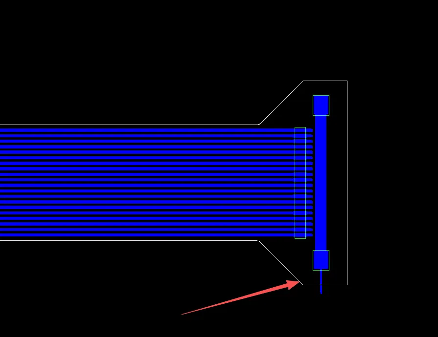
Figure 3: adding a single temporary lead wire
| Plating Item | Specified | What We Can Hold | Note |
|---|---|---|---|
| Hard Au | 1 µin | 0.8–1.5 µin | Needs continuous path or temporary lead |
| Ni underlayer | 120 µin | 100–150 µin | Standard barrier thickness |
| Isolated pads | 2 | Lead-wire solution | One temporary lead proposed |
In-House Panelization and Single-Piece Shipping After SMT
This part is a long, narrow flex strip. We planned to do the SMT assembly in-house. The customer had not supplied a preferred panel layout, so we proposed to panelize it ourselves, assemble on the panel, then singulate and ship individual pieces. Shipping large, thin panels after assembly raises the risk of handling damage. Single-piece shipping is cleaner for a 0.1 mm base material once components are on board.
Laser outline cutting happens after assembly and stiffener attachment. We set the laser parameters for the actual thickness in each zone. That only works reliably when the stiffened thickness is both known and held inside the agreed window.
Incoming Checks, Lamination Settings, and Thickness Mapping
Before releasing the job we looked at three things:
- Incoming thickness of the PI film and adhesive (micrometer checks on every lot).
- Lamination pressure, temperature, and time set to hit the 0.30 mm centerline with the agreed tolerances.
- Thickness mapping on every production panel at both the finger end and the connector end, with control limits set to the proposed ±0.03 mm and ±0.05 mm windows.
First-article cross-sections confirmed continuous adhesive fill, no voids, and actual measured thickness inside the windows. Hard-gold coupons with the temporary lead were also sectioned. Gold and nickel thicknesses met the 1 µin / 120 µin call-out, and lead removal left a clean pad with no residual copper or undercutting.
Once the stiffener thickness was corrected to a value that could actually reach 0.30 mm, both the dimensional and plating processes sat comfortably inside normal capability. No special equipment was required—only the right material choice and the right process settings.
| Process Step | Original Risk | What We Changed | Result |
|---|---|---|---|
| Stiffener total thickness | 0.1 mm PI cannot reach 0.30 mm | Thicker PI + adhesive; zone-specific tolerances | 0.30 ± 0.03 / ±0.05 mm held |
| Hard-gold isolated pads | No current path | Temporary lead on one pad | Uniform 1 µin Au / 120 µin Ni |
| Laser outline after assembly | Unknown thickness step | Laser settings matched to actual zones | Clean edge, no delamination |
First-Article Thickness, Cross-Section, and Gold Verification
We built first-article panels with the adjusted stiffener. Thickness was checked at multiple points along the finger zone and the connector zone with both a micrometer and a non-contact laser gauge. Every reading fell inside the proposed bands. Cross-sections showed solid adhesive fillets and no voids at the PI-to-FPC interface.
Hard-gold thickness was verified by XRF on both the bus-connected and the lead-wired pads. Results met the 1 µin Au / 120 µin Ni specification. After the lead was removed the pad surface was clean—no residual copper, no undercutting of the nickel.
Laser-formed edges looked clean under magnification. The transition from the 0.10 mm flex region to the stiffened region showed no carbon residue or fiber pull-out when the laser was set to the measured local thickness. The revised process window proved both achievable and repeatable for this quantity.
Final Construction and Release After Thickness Clarification
The original 0.1 mm PI stiffener and the 0.30 mm total-thickness call-out could not be built together. By moving to zone-specific finished thicknesses of 0.30 ± 0.03 mm at the finger end and 0.30 ± 0.05 mm at the connector end, and by adding one temporary lead wire for the isolated hard-gold pad, every requirement moved inside a stable process window. Once the customer confirmed the changes, we selected the correct stiffener materials, locked the lamination parameters, and ran the electrolytic gold process under normal conditions.
The takeaway is simple. Thickness numbers on an FPC drawing have to match the sum of the materials that are actually listed. When they do not, early clarification is the only way to keep both dimensional accuracy and plating quality under control. The final construction met the mechanical needs of the gold-finger and connector interfaces while staying fully inside the demonstrated capability of the rolled-copper FPC, PI stiffener, and hard-gold processes.
FAQ
Q1: Why can't a 0.1 mm PI stiffener produce a 0.30 mm total FPC thickness?
A 0.1 mm base plus a 0.1 mm PI film, even with adhesive, finishes around 0.18–0.22 mm after cure. The materials listed simply do not add up to 0.30 mm. To reach that number you need a thicker PI film or an extra reinforcing layer chosen so the final stack lands on target inside normal process tolerances.
Q2: Why use different thickness tolerances for the finger end and the connector end?
The gold-finger or contact zone usually mates with a precision connector that expects a tight thickness window. Holding ±0.03 mm there protects contact force and mating reliability. The connector end can live with ±0.05 mm without functional trouble, which gives the process more margin and better yield while still hitting the 0.30 mm nominal.
Q3: Why does an isolated pad need a temporary lead wire for hard-gold plating?
Electrolytic gold needs a continuous current path from the plating bus. An isolated pad gets almost no current and ends up with little or no gold. A temporary lead restores the path. After plating the lead is removed, leaving a fully finished pad. This is the standard way to keep hard-gold thickness uniform on isolated features.
Q4: How does laser forming react to thickness steps on a stiffened FPC?
Laser focus and power are set for the local material thickness. An unexpected step from 0.10 mm flex to a thicker or thinner stiffener zone can leave incomplete cuts, carbon residue, or edge delamination. When the stiffened thickness is known and held inside a defined window, the laser can be calibrated for each zone and the cut stays clean.
Q5: What thickness window can we realistically hold on an FPC-plus-PI stack?
With a properly chosen PI film and adhesive, a controlled lamination process can hold roughly ±0.03 mm to ±0.05 mm around a 0.30 mm centerline. Tighter windows raise process sensitivity and cut yield. Wider windows can cause mechanical fit problems. The tolerances we proposed balance functional need against what the process can actually deliver day after day.
Q6: Why ship the assembled FPC as single pieces instead of in panel form?
After SMT the long, narrow flex becomes more fragile. Building on a panel and then shipping individual pieces reduces the chance of bending or edge damage during transit. For a thin 0.1 mm base this is the cleaner approach, especially on low-quantity builds.