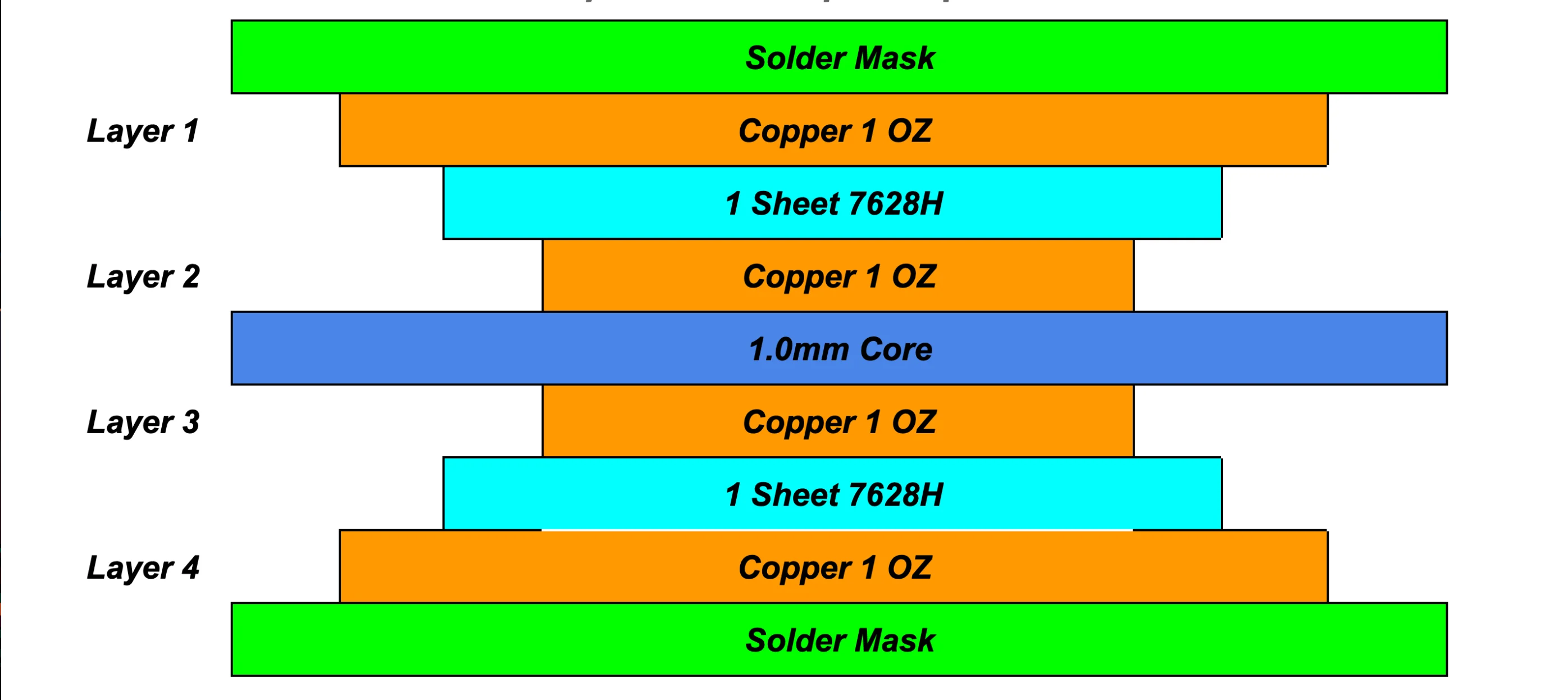
A PCB stackup is the construction the shop is being asked to press: layer order, core or prepreg at each interface, dielectric thickness, copper thickness, and the finished thickness on the drawing. Lamination is the press process that bonds the cores and prepreg into the specified construction. Most stackup questions in CAM start when those terms do not agree across the package, or when the inner-layer copper files do not look like the construction the press is being asked to run.
The usual mismatches are familiar. The stackup drawing and a later lamination figure name different cores, dielectrics, copper weights, or finished thicknesses. A stackup already confirmed on an earlier turn sits next to a new press figure in the same ZIP. Inner layers come in as traces and isolated lands with little or no pour, so after etch the prepreg has a lot of open relief to fill. The drawing calls a finished thickness and a copper thickness that the construction on hand may not both meet. How many copper files arrived only gives the layer count. A 4-layer PCB stackup and an 8-layer PCB stackup both still need those terms named at each interface.
The three EQs below are examples from recent packages, not a complete list and not a claim that every job fails in the same three places. One package still held a stackup we had already confirmed; production attached a different press figure and asked us to use that one. On another, L3 and L6 were traces and isolated lands only — no copper pour — so after etch those layers were mostly open. On a third, the lamination drawing called 2.2 mm finished thickness and 2 oz copper, and the note that came back offered 2.65 mm ±10% and 1 oz instead, because the thinnest 2 oz core in that review was 0.11 mm without copper, the dielectrics on the drawing sat thinner than that press would support, and 2 oz on the released line/space took out too many copper bridges.
| What we saw in the files | Where the files disagree | What the EQ asked |
|---|---|---|
| A previously confirmed PCB stackup and a later lamination figure in the same package | Layer order, core versus prepreg, dielectric thickness, copper thickness, or finished thickness no longer line up | Use the new press figure as the lamination construction, or keep the stackup already confirmed |
| L3 and L6 released as traces and isolated lands only — no copper pour | After etch those layers are mostly open; prepreg still has to fill that relief at press | Add pour where we show it, redesign the layers, or accept the sparse artwork in writing |
| Lamination drawing calls 2.2 mm finished thickness and 2 oz copper | A press from the cores and prepreg on hand lands at 2.65 mm ±10%; 2 oz on the released line/space takes out copper bridges | Keep finished thickness first and run inner and outer copper at 1 oz, or say which of those terms may move |
PCB Stackup and Lamination Construction in the Released Package
The PCB stackup drawing, the lamination figure, the notes on finished thickness, copper thickness, and material, and the Gerber copper files in layer order all sit in the same package. They can agree. When they do not, the first question is which of those files still owns the construction.
A stackup already signed on an earlier turn does not drop out just because a new figure showed up in the ZIP. Shops redraw a press figure for ordinary reasons — the core on the drawing is not what they can buy, one dielectric is thinner than they will press, the stack is not symmetric, the thickness target will not land. That is one common reason an EQ appears.
How many copper files arrived only gives us the layer count. Four layers or eight, each interface still has to say core or prepreg, with a dielectric thickness and a copper thickness on that line. The artwork will not choose the press for us. Until one document is confirmed as controlling, the layup remains open.
Core Thickness, Prepreg Thickness, and Copper Thickness on the Layer Stackup
Read the stackup drawing for layer order, core thickness, prepreg thickness, dielectric thickness, copper thickness, and the finished thickness it wants. Then open each copper file and see what actually flashed: a plane, a mixed layer, or traces and isolated lands. Residual copper is that flashed metal against the outline. We leave it as a picture of the layer. This review does not turn it into a shop percentage.
That pairing still leaves several things open: which core comes off the shelf, how far the prepreg slumps once it has filled the etched pockets, whether the called finished thickness will come out of the press, and whether the called copper thickness will etch on the line/space that was released. If a core note says 0.11 mm without copper, that is how we read that package. Inner copper is the foil on the core. Outer copper on the finished board may already include plating. Those stay two called numbers.
Finished thickness is the cores, the prepreg after press, and the copper. Change one and the other two shift. That is why a later press figure, sparse inner layers, and a thickness-versus-copper-weight offer tend to hang off the same reading. On the 2.2 mm / 2 oz job we lined each copper file up with its stackup line — L3 and L6 first — and wrote down the called copper thickness against the line/space on those layers, and the called finished thickness against the construction we would have to press.
| What the drawing and the copper files show | What still has to be confirmed |
|---|---|
| Layer order on the stackup drawing versus how many copper files arrived | Which document owns the press when a later figure does not match the confirmed stackup |
| Called core thickness, prepreg thickness, dielectric thickness, and finished thickness | Which core comes off the shelf, and how far the prepreg slumps after it fills the etched relief |
| Called copper thickness on each line of the stackup | Whether 2 oz will etch on the released line/space without taking out copper bridges |
| Whether L3 or L6 flashed as a plane, a mixed layer, or traces and isolated lands | Whether pour may be added, and where it has to stay off the released nets |
| Whether a core-thickness note is dielectric-only or includes copper — read as written | Whether 2.2 mm will come out of the construction the shop is prepared to press |
A Confirmed PCB Stackup That Does Not Match the Lamination Construction
On one of those example jobs we had already confirmed a stackup. Then a different lamination figure arrived with a request to press that one. Two constructions sat in the same package. Gerber copper does not break the tie. Line up layer order, core versus prepreg, dielectric thickness, copper thickness, and finished thickness on both documents and write down where they diverge.
When that EQ said the dielectric was too thin to laminate, it was talking about the released construction against the materials we were prepared to press on that job. That is not a published floor, and it is not a rule we copy onto the next board. The new figure is an offer. It does not overwrite the confirmed stackup on its own.
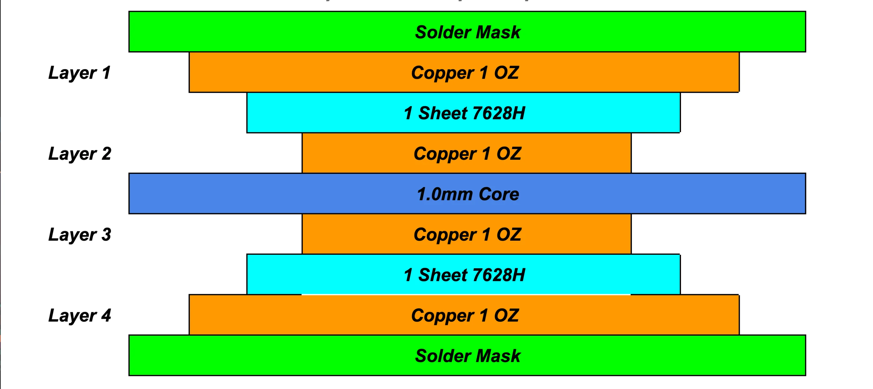
The question we send is which document controls. If the new figure is accepted, it becomes the lamination construction for any pour question and copper-thickness question that follow on that job. If it is not, the confirmed 4-layer PCB stackup stays the press instruction and the later figure comes off the job.
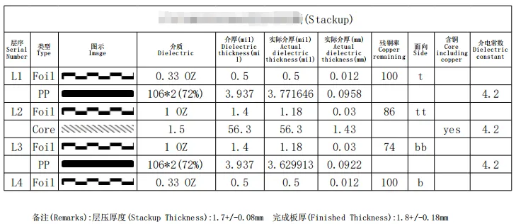
Updated 4-layer PCB stackup
Inner-Layer Residual Copper on the PCB Stackup During Lamination
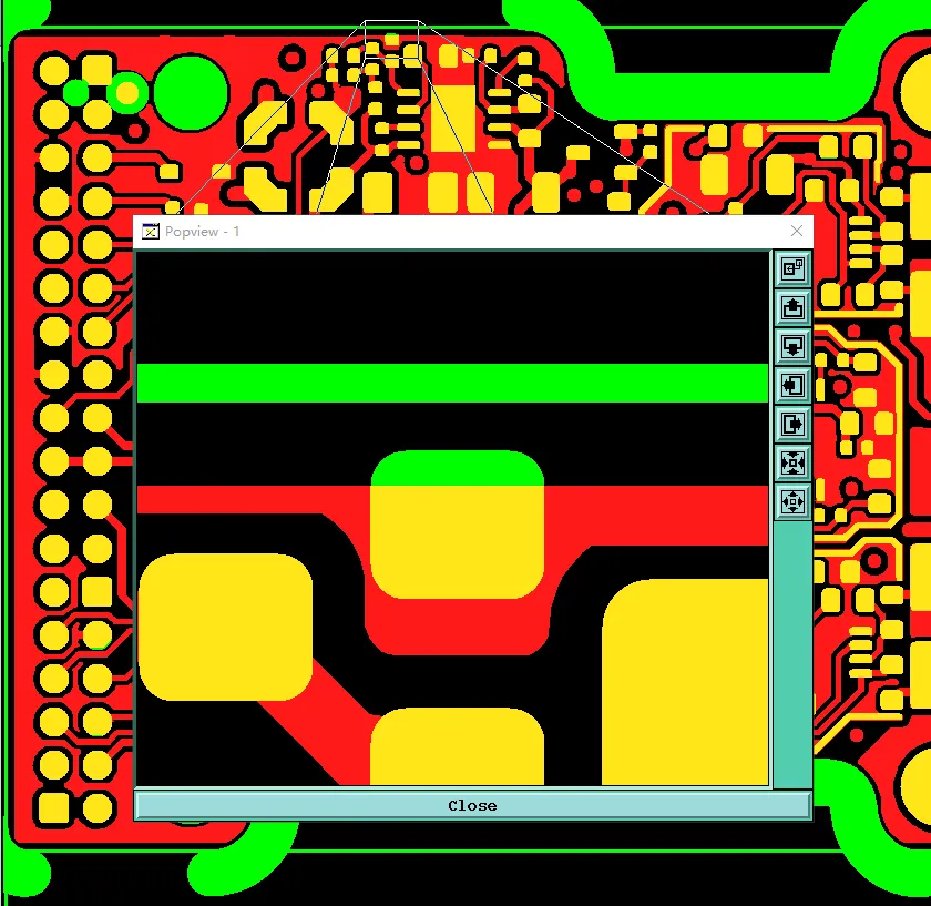
Agreeing the 8-layer PCB stackup drawing does not finish the review if an inner layer is almost empty. On the example job, L3 and L6 came in as traces and isolated lands only. There was no copper pour. Open the copper against the outline and the plane is simply not there — not a missing file, just artwork that left most of the layer open after etch. Other packages show the same condition on different layer numbers.
Prepreg resin has to fill that relief and still leave a bond line. That changes the resin distribution through the stack and can affect pressed thickness and lamination behavior. Depending on the construction and process, sparse copper distribution can also contribute to concerns such as resin-rich areas, voiding, or delamination. The same open layer can also pull pressed thickness down and unbalance the stack. Those ride with the artwork; they are not a separate warpage review.
The neighboring layer matters too. Sparse against sparse is a different fill than sparse against a plane. Added pour is one way to close the EQ, not the way we apply on our own. Any copper we add has to stay off the released nets and off isolation the designer left open. If we propose pour, we show where it would go. The customer then takes that pour, redesigns the layers, or accepts the sparse artwork in writing.
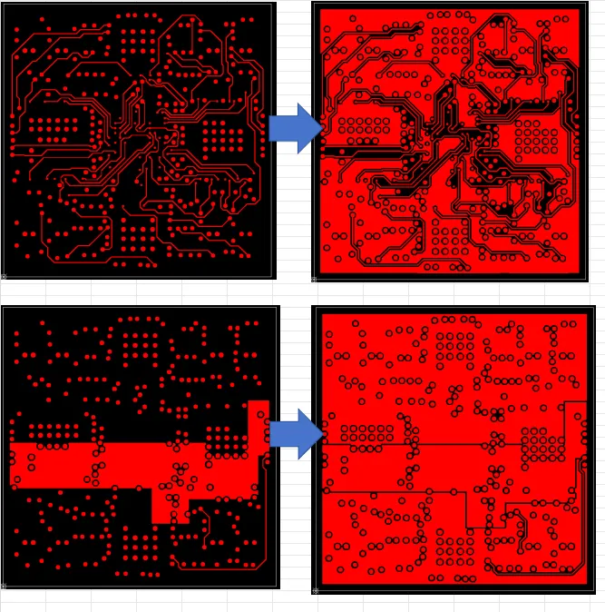
Adding copper pours on L3 and L6 layers by clearing 5mil from the original graphics on each side to increase the copper residual ratio and prevent resin starvation and board blistering during lamination
Dielectric Thickness and Copper Thickness When the Drawing Calls 2.2 mm
On the thickness example, the lamination drawing called 2.2 mm finished PCB thickness. The EQ started from the thinnest 2 oz core in that review — 0.11 mm without copper — and from the statement that the dielectrics on the drawing sat thinner than that press would support without a delamination risk. Build from the cores and prepreg we were prepared to use, and the thickness in the note became 2.65 mm ±10%. That figure belongs to that job. It is not a general finished-thickness spec.
The same note also called 2 oz, and the flashed line/space was tight. Etching 2 oz, as written there, took out too many copper bridges — the etch remainder between features. The factory offer was to keep finished thickness first and run inner and outer copper at 1 oz. That changes copper thickness, resistance, and any impedance that assumed 2 oz. It is an edit to a released call, so it stays in the EQ.
Dielectric thickness, finished thickness, and copper thickness move together. Signing one of them leaves the other two open. We take finished thickness and copper thickness from the drawing, compare the called copper weight with the line/space on the inner and outer Gerber, and put the EQ offer on the table as a complete substitute when that is what was proposed. On that job the offer was 2.65 mm ±10%, 1 oz, and the new lamination figure if it belonged to the same note. Then we ask which requirement may move — thickness, copper thickness, or both.
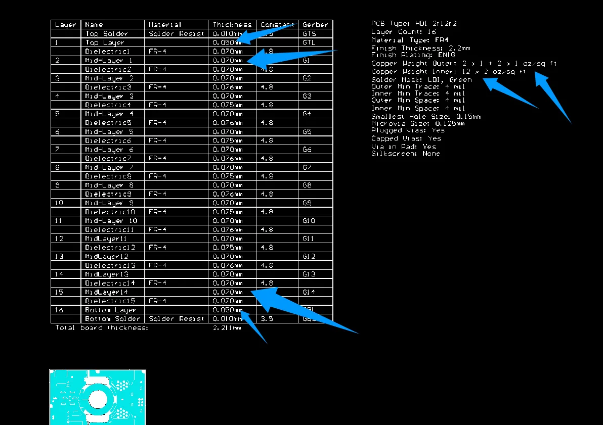
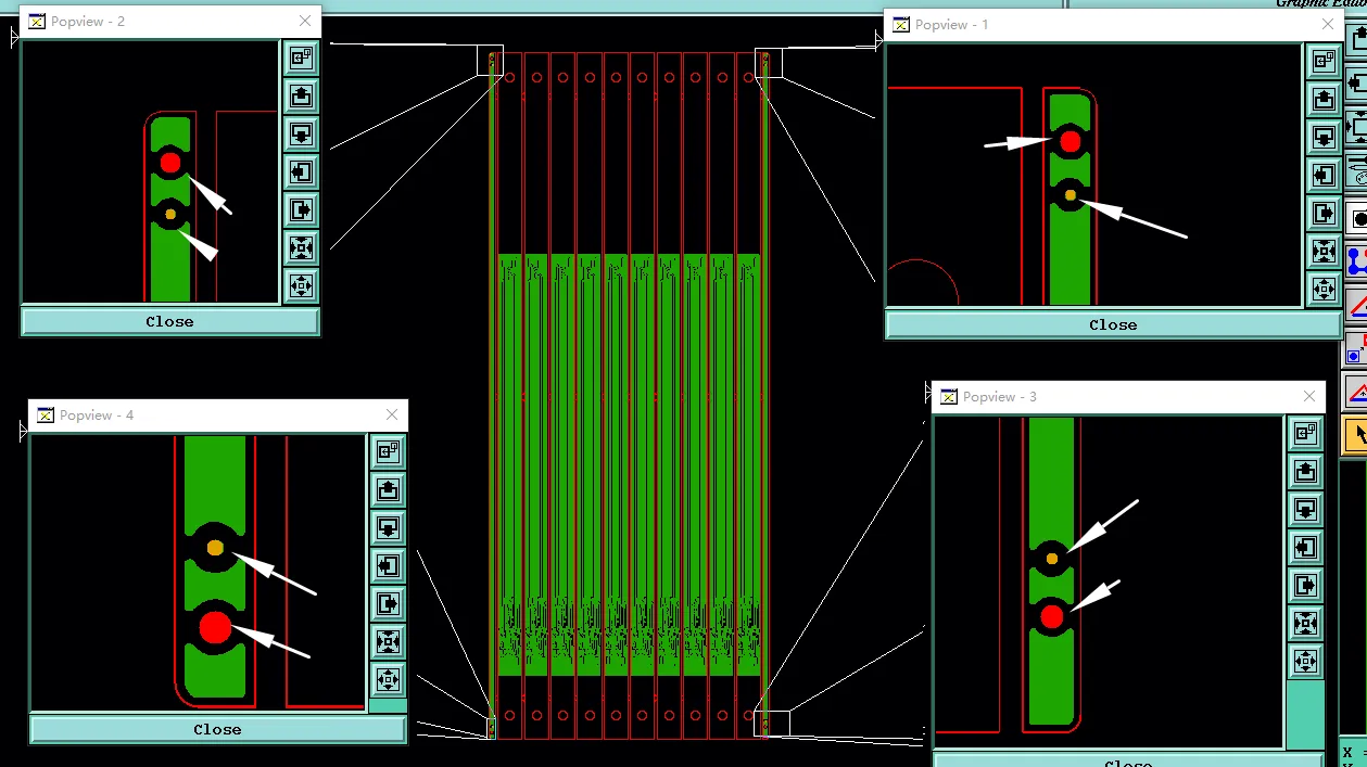
The dielectric thickness of your lamination structure is relatively thin, which may cause delamination during lamination.
Keep the Released PCB Stackup or Confirm the Lamination Construction
The close is the written answer to the confirm request. Each path names the file that still owns the job. Mixed answers are fine: keep the confirmed stackup and add pour on the sparse layers; take the new press figure and keep the called copper weight; drop copper weight only on the layers that will not etch as drawn. A partial close still has to name the revised note and the revised Gerber layer. Everything it leaves unnamed stays as released.
| Path | What stays as drawn | What the close allows us to change | What lamination then uses |
|---|---|---|---|
| Keep the released PCB stackup | Confirmed stackup, 2.2 mm / 2 oz, and L3/L6 as flashed | The later lamination figure comes off the job; press-risk language already in the EQ is recorded against that keep | The confirmed layer stackup drives layup. Sparse inner layers stay as released. |
| Accept the alternate lamination construction | Gerber copper, except any pour the same close also names | New press figure plus the EQ outcome the customer signs — 2.65 mm ±10%, 1 oz, or the subset they accept | One stackup drawing then drives incoming material, layup, and finished thickness. |
| Change only the conflicting term | Every line of the stackup the close does not name | Specified pour on L3/L6; or 1 oz only on layers that will not etch at 2 oz; or keep 2 oz and accept a different finished thickness | The revised note and the revised Gerber layer. Unnamed terms stay as released. |
Once that answer is in, there is one controlling layer stackup: order, core versus prepreg, dielectric thickness, copper thickness, and finished thickness. Sparse inner layers either stay as released or show the agreed pour. Gerber is not rewritten off the note, and the thickness note is not rewritten off the Gerber.
Before the package goes out, put the confirmed stackup next to any later lamination figure and next to the inner copper files. If those already disagree, write keep, accept the alternate, or change this term into the note. Leaving that choice out of the package is how an EQ of this kind starts. Until that line is written, the confirmed stackup, the called thickness and copper weight, and the inner-layer artwork stay as released.
PCB Stackup and Lamination Questions From CAM Review
Q1: What is a PCB stackup?
A1: The layer-by-layer construction on the released drawing: copper order, core or prepreg at each interface, dielectric thickness, copper thickness, and the finished thickness the drawing wants. The Gerber copper files sit on those lines. They do not stand in for the drawing.
Q2: What is PCB lamination?
A2: The press that bonds the cores and prepreg into that stackup. The lamination construction — the press figure — is what layup follows. When a later figure disagrees with a confirmed stackup, the press waits on which document owns the job.
Q3: What is the difference between core thickness and prepreg thickness?
A3: A core arrives already cured, with copper on it. Prepreg is the B-stage sheet that flows and fills at press. They are separate lines on the drawing. Finished thickness is both of them after press, plus the copper.
Q4: What is dielectric thickness in a PCB stackup?
A4: The insulator between two copper layers, as written on the stackup drawing. Whether that number is a core, a prepreg stack, dielectric-only, or inclusive of copper depends on the note. The 0.11 mm 2 oz core without copper in one EQ is that package's wording, not a catalog value.
Q5: What is copper thickness on a PCB stackup?
A5: The copper weight called on each line of the drawing. Inner copper is foil on the core. Outer copper on the finished board may already include plating. A call for 2 oz is not automatically the same number after etch and after plate, and it still has to live with the released line/space.
Q6: What is residual copper on an inner layer?
A6: The copper left on that Gerber layer after etch — flashed features against the outline. On one example job L3 and L6 were traces and isolated lands only, so most of each layer was open. This review does not publish a residual-copper percentage as a factory limit.
Q7: Why does low residual copper matter during lamination?
A7: Prepreg resin has to fill the open relief and still leave a bond line. That is the concern behind resin starvation, voids, and delamination on sparse inner layers. The same artwork can also pull pressed thickness down. Added pour is a close the customer confirms, not an edit we apply on our own.
Q8: Does a 4-layer PCB stackup use the same lamination construction as an 8-layer PCB stackup?
A8: Layer count only tells us how many copper files arrived. Each interface still needs core or prepreg, dielectric thickness, and copper thickness named. We do not drop in a standard 4-layer or 8-layer build in place of a missing or conflicting drawing.
Q9: Who decides finished board thickness versus copper thickness when they conflict?
A9: The customer, in a written close that names the stackup drawing or the new lamination figure, the finished thickness, and the copper thickness on the layers that change. On the job that called 2.2 mm and 2 oz, the EQ offered 2.65 mm ±10% and 1 oz as one substitute. Signing thickness alone leaves copper thickness open, and the other way around. Until that line is written, the released stackup stays as drawn.