In PCB fabrication, even straightforward 4-layer designs can trigger multiple engineering questions (EQs) during CAM review. This case study examines a recent 4-layer FR-4 order (#FR4-20260130-038) with dimensions 162 × 73 mm, 1.6 mm target thickness, and ENIG surface finish. The project highlighted common disconnects between design intent and manufacturing realities, particularly around stackup construction, countersink hole processing, and core material availability.
As a senior CAM engineer with over 15 years in the industry, I've seen how these seemingly minor discrepancies can cascade into production delays or quality issues. Our engineering team raised several EQs to align the fabrication data with actual factory capabilities before releasing the job to production.
Order Overview
This was a standard 4-layer PCB using FR-4 material with TG170 rating. The board measured 162 mm × 73 mm, with a specified finished thickness of 1.6 mm. Copper weight was 1 oz on both outer and inner layers. Minimum hole size was 0.15 mm, and the design required 100% flying probe testing. Surface finish was ENIG (immersion gold), with no impedance control specified. Panelization was 1×1 single piece, quantity 20 pcs. The customer requested countersink holes and specific stackup configuration.
Production type was mechanical forming, with no V-cut or scoring initially noted. While the design appeared routine, the CAM review quickly revealed inconsistencies in board thickness requirements, stackup details, and hole processing specifications that required clarification to prevent manufacturing risks.
Main Engineering Questions Found During CAM Review
Stackup and Board Thickness Inconsistencies
The most significant issue involved board thickness and stackup construction. The original customer data called for 1.6 mm finished thickness, but the provided stackup details showed deviations in core material thickness. We noticed the specified 1.5 mm core (copper-free) was not a standard stocked item in our inventory.
![]()
Figure 1: 1.6 mm finished thickness for original customer data
Our engineer suggested updating the stackup after reviewing the provided lamination diagram. The initial confirmation for 1.6 mm proved inconsistent with available materials. We proposed alternatives: a 1.53 mm core or 1.43 mm core, both without copper cladding, to maintain the target thickness within acceptable tolerances.
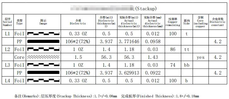
Figure 2: Updated stackup
Later, an updated stackup for 1.8 mm ±10% was shared for confirmation. This deviation was substantial enough to affect overall board flatness and subsequent processes like drilling and plating. If ignored, the mismatch could lead to excessive board warpage or delamination during reflow in assembly, especially with TG170 material under thermal stress.
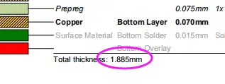
Figure 3: Updated stackup for 1.885mm total thickness
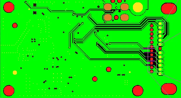
Countersink Hole Depth and Placement
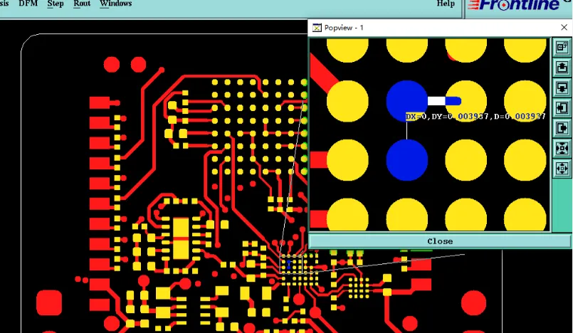
Four countersink holes required special attention. The customer specified a depth of 1.35 mm based on their parameters.

Figure 4: Four countersink holes needed to be processed as copper-plated holes.
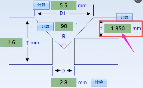
Figure 5: 1.35mm countersink hole
We calculated and confirmed the depth against the 1.6 mm board thickness. Importantly, these holes were positioned directly on copper areas and needed to be processed as copper-plated holes.
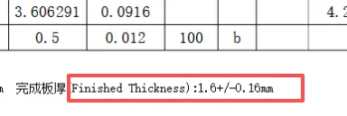
Figure 6: 1.6 mm board thickness confirmation
Our CAM team identified that manufacturing countersink holes on copper pads requires precise depth control to avoid breaking through the copper or leaving insufficient plating. We confirmed the processing method and provided visual references for the expected outcome. Had this not been clarified, the risk of exposed copper at the bottom of the countersink or incomplete plating could have caused poor solderability or mechanical weakness in assembly.
Drill Tolerance and Manufacturability Concerns
The design included strict drill tolerances that our process engineers flagged as challenging to control consistently. Tight tolerances on smaller holes (0.15 mm minimum) combined with countersink features increase the risk of drill wander or breakout, particularly in a 4-layer construction.
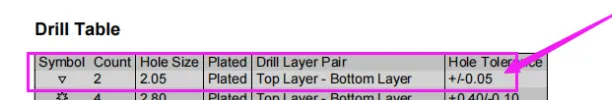
Figure 7: Strict drill table
We recommended reviewing these tolerances against standard manufacturing capabilities. According to IPC-6012 Class 2 guidelines commonly applied in such cases, overly stringent tolerances can drive up scrap rates without adding functional value.
Suggested EQ Categories
Stackup & Material Issues
- Core material thickness availability (1.5 mm non-standard)
- Finished board thickness confirmation (1.6 mm vs. updated 1.8 mm options)
- Lamination structure deviation from initial customer data
Hole & Tolerance Issues
- Countersink hole depth calculation and verification (1.35 mm)
- Strict drill tolerance control feasibility
- Countersink placement on copper features
File & Manufacturing Data Issues
- Overall fabrication data confirmation
- Stackup diagram updates and alignment
Manufacturing Risks and DFM Insights
This case underscores several recurring DFM challenges in multilayer PCB production. Non-standard core thicknesses often force material substitution discussions. In this instance, proceeding without confirming the stackup could have resulted in boards outside the customer's mechanical envelope, leading to assembly fit issues or signal integrity problems in the final product.
Countersink holes on copper areas are particularly risky. If depth control is off by even 0.1 mm, it can expose underlying dielectric or damage the copper ring, causing open circuits or cosmetic defects that fail IPC-A-600 inspection. Our experience shows that such features require explicit confirmation because automated depth control in mechanical countersinking has inherent process variation.
Tight drill tolerances compound these risks. Without adjustment, we could see increased hole breakout, plating voids, or via cracking after thermal cycling — all of which contribute to lower yields and higher costs passed on to the customer.
How the Engineering Team Resolved the Issues
Our team worked iteratively with the customer. After the initial stackup review, we provided updated lamination diagrams showing viable material options (1.53 mm and 1.43 mm cores). The customer selected a configuration, and we adjusted the target thickness accordingly.
For the countersink holes, we confirmed the 1.35 mm depth calculation and processing sequence (drill then countersink with copper protection). We also relaxed non-critical tolerances slightly within acceptable limits to improve process capability while maintaining functional requirements.
Throughout the process, we maintained clear visual references and calculation sheets. This collaborative approach is standard in our CAM workflow to minimize risk before production release.
Final Manufacturing Outcome
All engineering questions were resolved through updated stackup confirmation, countersink processing parameters, and material selection. The CAM data was revised accordingly, and the order was approved for production with 1.6 mm target thickness using the agreed core material. The job proceeded without further issues.
Key Takeaways for PCB Designers
- Always specify exact core material thicknesses and confirm availability with your fabricator early, especially for non-standard values like 1.5 mm copper-free cores.
- Provide detailed stackup drawings with copper weights, dielectric thicknesses, and tolerance notes before final Gerber submission.
- For countersink or special holes, include depth requirements, placement relative to copper, and expected cross-section views.
- Review drill tolerance specifications against the fabricator's process capabilities — overly tight tolerances increase cost and risk without benefit.
- Ensure layer stackup in design software matches the final fabrication notes to avoid thickness mismatches.
- Consider panelization implications even for small runs, as it affects material utilization and mechanical stability.
- Document any mechanical features (countersinks, slots) clearly in both Gerber files and fabrication drawings.
FAQ
Q1: Why is core material thickness availability such a common issue in multilayer PCBs?
A1: PCB factories stock standard core thicknesses for efficiency. Non-standard sizes like 1.5 mm require special procurement, which extends lead time and may affect final board thickness tolerance. Confirming alternatives early prevents delays.
Q2: What risks arise from unconfirmed countersink hole depth?
A2: Incorrect depth can lead to exposed copper, damaged pads, or insufficient mechanical strength. In severe cases, this causes assembly failures or shorts after component mounting. Precise confirmation ensures proper plating and depth control.
Q3: How do stackup deviations affect PCB performance?
A3: Variations in dielectric thickness impact impedance (if controlled), warpage, and reliability under thermal cycling. In this case, the shift from 1.6 mm to alternatives required careful review to maintain mechanical and electrical integrity.
Q4: Why do CAM engineers pay close attention to drill tolerances?
A4: Tight tolerances increase the chance of drill breakage, misalignment, or breakout, especially near copper features. This directly affects yield and can cause open or short circuits. Balancing tolerance with process capability is key to reliable production.
Q5: Should designers always use standard material thicknesses?
A5: Yes, whenever possible. Standard cores reduce cost and lead time. When custom thicknesses are needed, early communication with the manufacturer allows for suitable compromises that meet both design and manufacturing requirements.
Q6: What is the benefit of detailed EQ communication before production?
A6: It prevents scrap, rework, and delays. In this case, proactive clarification ensured the boards met mechanical and quality standards, avoiding potential issues like warpage or plating defects.