Ultra-thin 0.4mm 4-layer PCBs with dense BGA areas and special marking requirements often push solder mask and process limits during CAM engineering review. This case reviews a compact 29.46 × 30.23 mm board using TG170 FR-4 material with blind vias and resin plugged holes. Multiple critical DFM issues were identified that required detailed customer clarification before production.
As a senior CAM engineer, I routinely see tight-pitch designs on thin boards create significant manufacturability challenges. In this order, the combination of fine BGA spacing, conflicting documentation, and custom marking needs triggered several Engineering Questions (EQs). Our team focused on preventing solder bridging, ensuring accurate markings, and verifying stackup compatibility.
Order Overview
This 4-layer FR-4 board ( #FR4-20260331-072 ) featured TG170 material, 0.4mm finished thickness, and 1oz copper on inner and outer layers. The design included ENIG surface finish, 0.15mm minimum hole size, green solder mask, white silkscreen, blind vias, and resin plugged holes. Production required 100% flying probe testing, 2x2 panelization with 4mm process edges, V-scoring, and mechanical forming. Quantity was 20 pieces.
Customer files included a PDF with additional requirements for serial numbers and potential QR code marking, making file consistency and DFM verification particularly important for this thin high-density board.
Main Engineering Questions Found During CAM Review
1. Tight BGA Pitch and Solder Mask Bridge Limitations
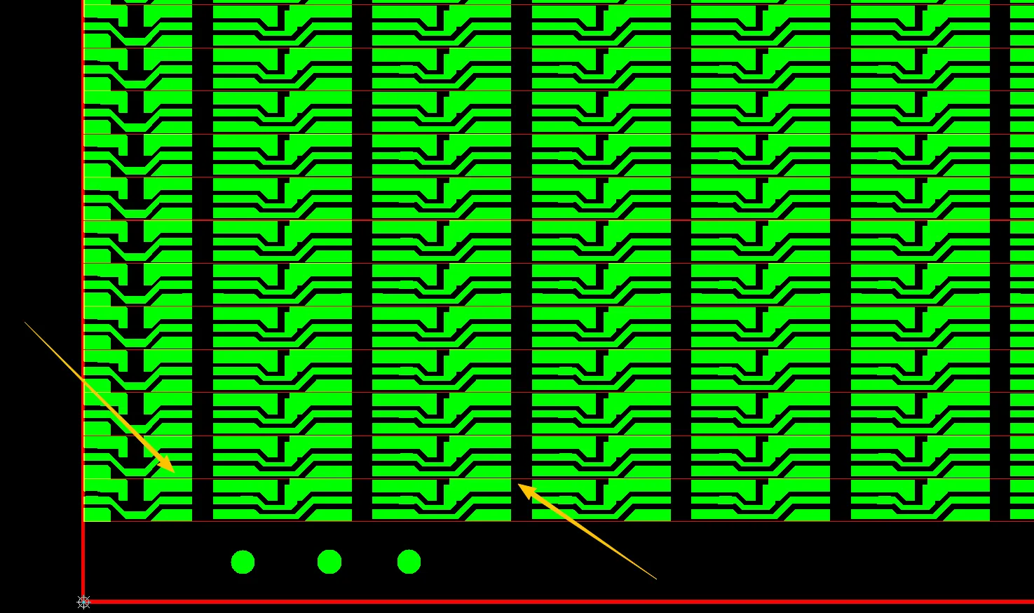
The most critical issue was the BGA pad spacing. The original design showed only 3.94mil pitch between pads. After standard solder mask expansion compensation, the effective spacing dropped to approximately 2.94mil, which is too tight to reliably form a solder mask bridge between pads.
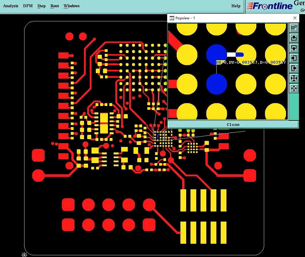
Figure 1: too tight to reliably form a solder mask bridge between pads
We noticed this during detailed solder mask and drill data analysis. Our CAM engineer raised an EQ because without a proper mask bridge, there is a high risk of solder bridging during SMT assembly. On a thin 0.4mm board with 1oz copper, the tight geometry further complicates reliable mask application and registration.
If this EQ had been ignored and production continued, the boards would likely suffer from frequent solder shorts between BGA pads, leading to assembly failures, rework, or complete scrap. In field use, such defects could cause signal instability or intermittent connections. According to typical IPC-A-600 acceptability criteria, this spacing falls below reliable solder mask dam capabilities for standard processes.
2. Serial Number and QR Code Marking Requirements
The order required adding sequential serial numbers from PN1 to PN20 on the boards. The customer provided a PDF with guidance on marking, which our team interpreted as placement instructions. However, the market side also requested a QR code, which would necessitate laser marking — a process that adds extra cost and requires specific confirmation.
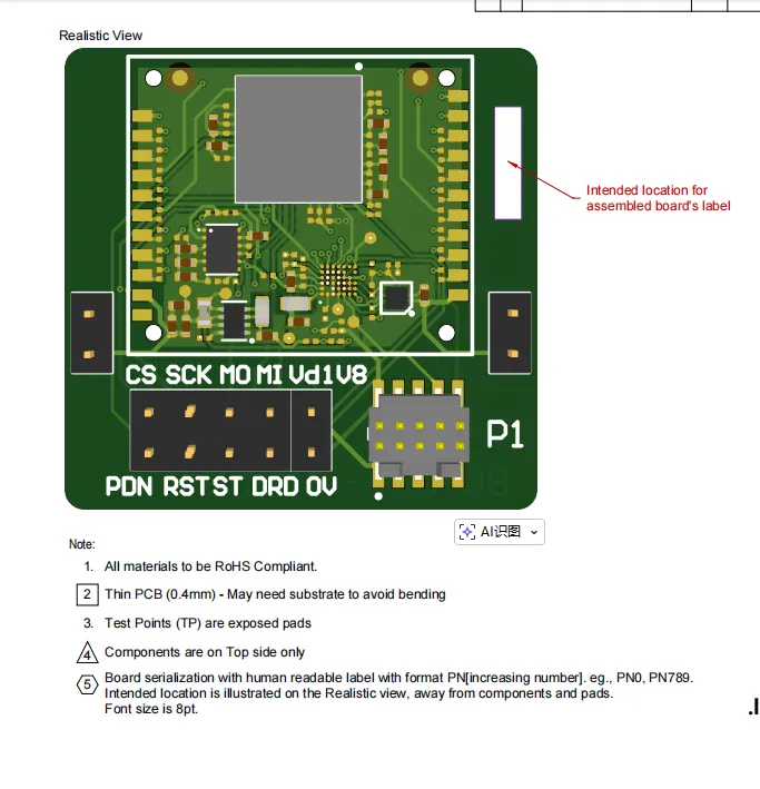
Figure 2: customer provided a PDF with guidance on marking
During file review, we noticed discrepancies between the PDF instructions and the standard order notes. Our CAM engineer raised an EQ asking the customer to confirm whether the serial numbers should be added by us choosing a suitable location, the exact layer, and whether the laser QR code was mandatory. Later follow-up from the customer specified a preferred position, which we verified against the board layout to avoid overlapping with other features or affecting solder mask/silkscreen areas.
We noticed that unclear marking requirements frequently cause version mismatches or misplaced identifiers. If left unconfirmed, serial numbers could be added in incorrect locations or omitted entirely, leading to traceability failures during quality control, customer incoming inspection, or field returns. Additionally, proceeding with laser QR code without cost confirmation could result in unexpected expenses or production delays. This type of ambiguity often triggers multiple review cycles before final approval.
After customer clarification on position (PN1 to PN20) and QR code decision, we updated the production files accordingly to ensure accurate and compliant markings.
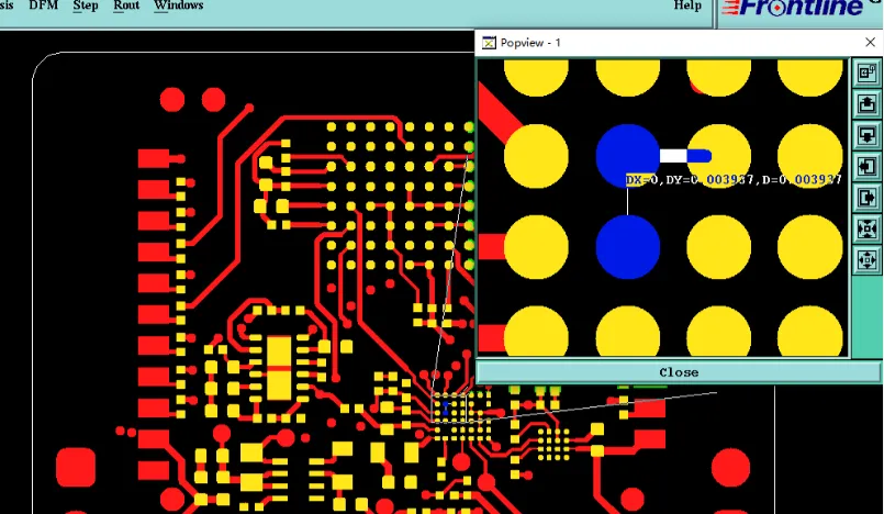
3. Stencil vs. Solder Mask Openings and Stackup/Thickness Confirmation
Several pads had solder mask openings defined, but the corresponding stencil (steel mesh) layer data did not match, with some openings missing in the stencil file. This mismatch could lead to incorrect solder paste volume during SMT assembly.
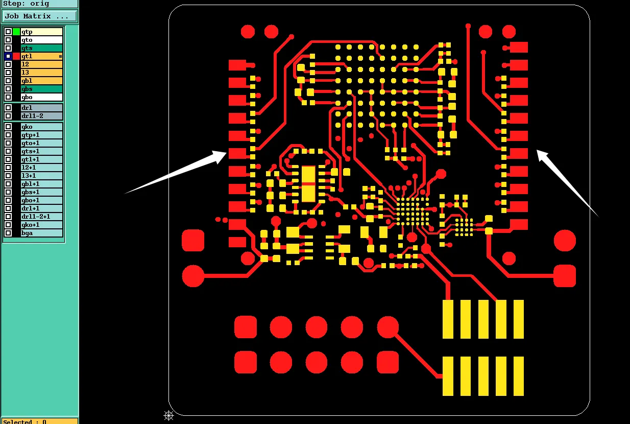
Figure 3: some pads have no opening on the corresponding steel mesh layer
Additionally, the provided PDF contained board thickness notes that conflicted with the specified 0.4mm finished thickness. We also asked the customer to confirm the lamination stackup diagram for this thin 4-layer build with blind vias.
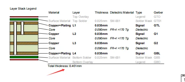
Figure 4: PCB stackup with 0.461mm board thickness
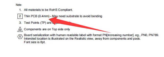
Figure 5: PDF contained board thickness notes that conflicted with the specified 0.4mm finished thickness
Our team identified these inconsistencies while cross-checking all output layers and documentation. We raised EQs to align the stencil data with mask openings and verify the final board thickness and stackup parameters, as even small deviations on a 0.4mm thin board can significantly impact mechanical fit, impedance (if applicable), and drilling/plating reliability.
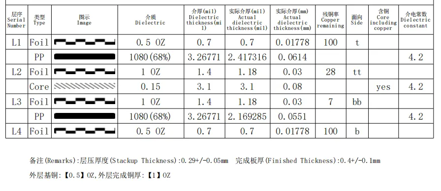
Figure 6: PCB stacup structure
If ignored, mismatched stencil data would likely cause insufficient or excessive solder paste, resulting in open joints, solder bridging, or tombstoning during assembly. Conflicting thickness information could lead to improper lamination pressure, board warpage, delamination, or finished boards out of specification. On thin high-density designs like this, such issues often result in high scrap rates and repeated engineering communication.
The customer confirmed the stencil openings and stackup, allowing us to finalize the production data with consistent parameters.
Suggested EQ Categories
Solder Mask & Silkscreen Issues
- Tight BGA pitch preventing solder mask bridge
- Stencil data mismatch on opened pads
Special Structure Clarification
- Serial number placement and QR code marking
- Stackup and board thickness consistency
Manufacturing Risks and DFM Insights
Dense BGA layouts on thin boards are a frequent source of DFM flags. Designers often specify pitches without considering solder mask expansion and bridge capability, leading to inevitable bridging risks during assembly.
If the BGA spacing issue had been ignored, high rates of solder shorts would have caused major assembly yield loss and potential field failures. Inconsistent documentation for markings and thickness further risks production errors and multiple revision loops.
How the Engineering Team Resolved the Issues
Our team provided annotated screenshots highlighting the tight BGA areas and recommended increasing pad spacing or adjusting mask settings where possible. For markings, we confirmed serial number positions on the appropriate layer and clarified the QR code cost. Stackup and stencil data were aligned after customer confirmation.
We noticed the stencil mismatch early and updated files accordingly. This collaborative process ensured all risks were mitigated before release.
Final Manufacturing Outcome
All EQs received clear customer confirmation. BGA parameters were optimized within limits, markings finalized, stackup approved, and production files updated. The order was released for fabrication after full DFM alignment.
Key Takeaways for PCB Designers
- Verify BGA pad pitch allows sufficient solder mask bridge (typically >4-5mil after compensation) on thin boards.
- Provide consistent documentation for board thickness, stackup, and special markings in both Gerber and PDF files.
- Coordinate stencil openings with solder mask data to avoid assembly mismatches.
- Clearly specify serial number ranges, positions, and any QR/laser marking requirements upfront.
- Account for thin board (0.4mm) registration and mask application tolerances in high-density designs.
- Be prepared for DFM adjustments on fine-pitch features and respond promptly to EQs.
- Include detailed fabrication notes for blind vias and resin plugging on multilayer thin boards.
- Perform pre-submission DFM checks focusing on solder mask and assembly compatibility.
FAQ
Q1: Why is tight BGA pitch a common DFM issue on thin PCBs?
A1: Solder mask expansion reduces the gap between pads. Below ~3mil effective spacing, reliable solder mask bridges cannot be formed, leading to high risk of solder shorts during assembly.
Q2: What risks arise from insufficient solder mask bridge on BGA?
A2: Solder bridging between pads, causing electrical shorts, assembly failures, rework, or scrap boards. This is especially problematic on thin high-density designs.
Q3: Why confirm serial number and QR code markings during CAM review?
A3: To ensure correct placement, layer, and processing method. Laser QR codes add cost and require specific confirmation to avoid surprises in production.
Q4: How important is stencil data consistency with solder mask?
A4: Critical for SMT. Mismatched openings can cause insufficient or excess solder paste, leading to poor joints or bridging.
Q5: What should designers do when PDF and Gerber specs conflict?
A5: Clearly indicate the authoritative source and confirm all details with the factory to prevent misinterpretation of thickness, markings, or features.