Ultra-thin 0.2mm 2-layer flexible PCBs with white solder mask and high-volume panelization frequently encounter manufacturability limits during CAM review. This case analyzes order involving a 64 × 600 mm board using pressed copper material. During engineering analysis, several critical DFM issues related to solder mask thickness, panel stability, and edge clearance required detailed customer clarification.
As a senior CAM engineer, I have handled many thin and flexible board projects. In this instance, the combination of 0.2mm finished thickness, white solder mask on both sides, and minimal process edges created multiple production risks. Our team raised targeted Engineering Questions (EQs) to align design intent with actual factory capabilities and prevent defects in downstream SMT and assembly.
Order Overview
This was a 2-layer flexible PCB ( #FPC-20260325-010 ) built on pressed copper material with 0.2mm finished thickness and 1oz copper on both layers. The design specified OSP surface finish, white solder mask on both sides, black silkscreen, 0.3mm minimum hole size, and 6mil line width/spacing. Production used full flying probe testing, V-scoring, laser forming, and a large 20×1 customer panelization with no process edges. Quantity was 100 pieces (5 sets).
The ultra-thin profile and flexible nature made this board particularly sensitive to solder mask application, panel handling, and edge protection during routing and scoring.
Main Engineering Questions Found During CAM Review
1. Solder Mask Thickness Conflict on Ultra-Thin 0.2mm Board
The customer required 1oz copper with white solder mask on both sides for a 0.20mm finished board thickness. However, standard white solder mask application adds approximately 15μm per side, making the total thickness unachievable within the specified limit.
We noticed this immediately during stackup and mask data review. Our engineer flagged it because exceeding the target thickness would violate the mechanical specification and potentially affect flexibility and impedance characteristics in this thin construction. We asked the customer to confirm whether to reduce mask thickness, switch to a thinner variant, or adjust the finished board tolerance.
If ignored, the board could end up thicker than specified, leading to assembly fit issues, reduced flexibility, or failure in final product integration. In extreme cases, excessive mask buildup on thin flex materials can cause cracking or delamination under bending stress.
2. No Process Edges on Large 20×1 Panel - Risk of Board Scattering
The panelization used a 20×1 configuration with zero process edges on both ends. Based on our production experience with long, thin flex panels, this setup makes the panel prone to scattering during handling, V-scoring, and especially SMT processes.
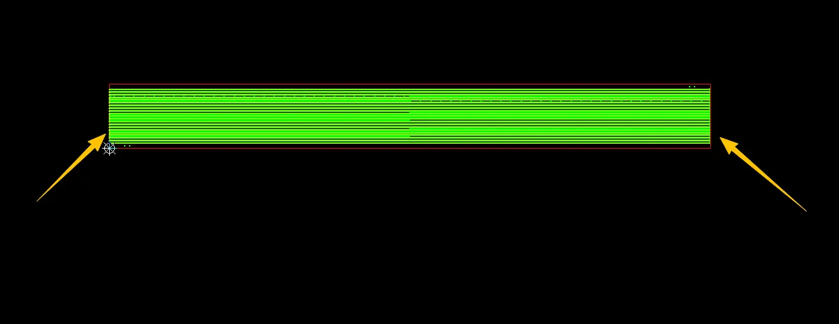
Figure 1: 20×1 configuration with zero process edges on both ends
We noticed the lack of connecting tabs or edges during panel file review. Our CAM team strongly recommended adding at least 5mm process edges on both ends to provide stability. The customer initially disagreed, prompting further discussion with annotated images showing potential handling risks.
If this had been ignored, individual boards could separate prematurely during manufacturing or SMT, leading to misalignment, dropped components, or complete production line stoppages. Scattered thin flex boards are also prone to edge damage and cosmetic defects.
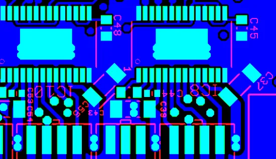
3. Trace-to-Outline Clearance and Silkscreen Issues
Traces on both sides were routed flush with the board outline edge. During CAM review of the outline and routing layers, we identified that V-scoring or laser cutting along the outline would directly expose copper, creating high risk of edge short circuits and board blackening (oxidation or resin smear) after depanelization.
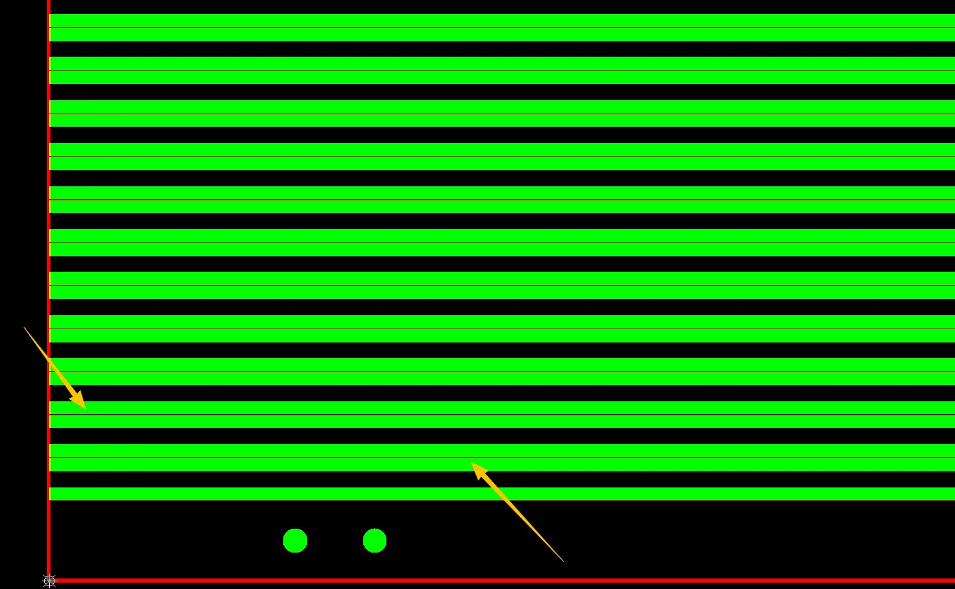
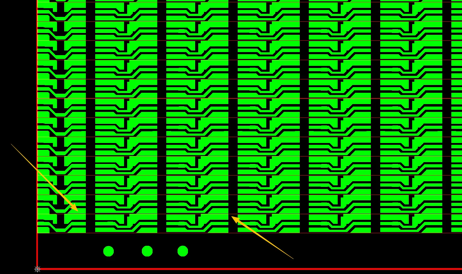
Figure 2, 3 : traces on both sides were routed flush with the outline edge
Our CAM engineer raised this as a critical concern because on flexible PCBs, especially with no process edges, insufficient clearance between copper features and the final outline frequently leads to manufacturing defects. We recommended increasing the trace-to-edge clearance to provide a safe margin for cutting and to protect against edge-related failures.
Additionally, some solder mask openings for silkscreen were positioned too close to pads, which could result in mask encroaching on or covering the pads during printing. On the bottom layer, a group of characters was designed with insufficient height, making them prone to blurry or incomplete silkscreen printing.
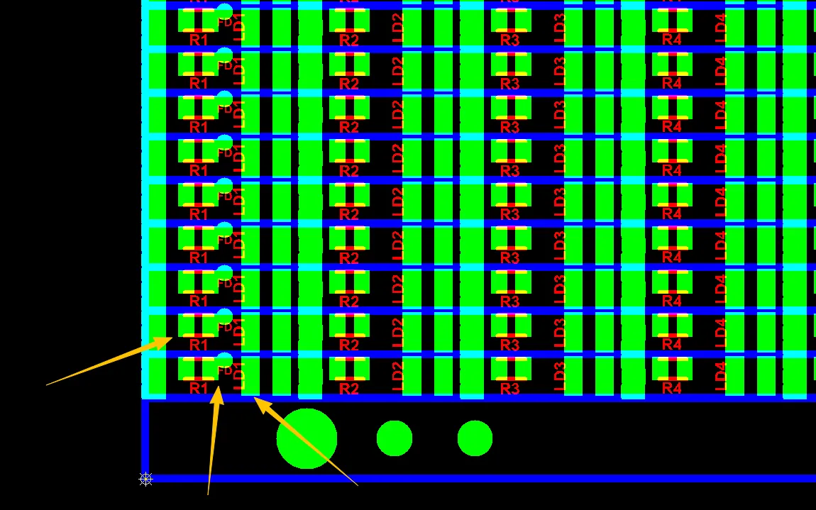
Figure 4: silkscreen openings near pads
We noticed these details while cross-checking the silkscreen, solder mask, and outline files. Our team provided magnified views and suggested adjustments to character size and opening positions. The customer later confirmed the changes, noting that the enlarged characters would print clearly.
If these issues had been ignored, production would likely result in exposed copper at the edges causing short circuits during assembly or field use, poor solderability, cosmetic defects like board blackening, and unreadable markings that complicate traceability and quality inspection. Such problems are common on thin flex boards and often lead to yield loss or customer rejection after SMT.
This confirmation and adjustment were essential to ensure reliable edge integrity and clear legibility of all markings.
Suggested EQ Categories
Stackup & Material Issues
- Solder mask thickness vs. ultra-thin 0.2mm board specification
Panelization & Process Optimization
- Absence of process edges on long 20×1 flex panel
- Recommendation for 5mm end tabs to prevent scattering
Solder Mask & Silkscreen Issues
- Trace-to-edge clearance and exposed copper risk
- Silkscreen character size and opening proximity to pads
Manufacturing Risks and DFM Insights
Ultra-thin flex boards demand careful balance between mechanical specifications and process capabilities. Designers often underestimate solder mask thickness contribution on 0.2mm boards or the handling difficulties of long panels without adequate tabs. The flush trace-to-edge design is a common oversight that frequently triggers EQs for edge protection.
Ignoring the process edge recommendation could lead to severe handling problems and high scrap rates during SMT. Similarly, insufficient trace clearance risks exposed copper after depanelization, potentially causing short circuits or corrosion-related failures in the field.
How the Engineering Team Resolved the Issues
Our team provided clear explanations with magnified images and calculations showing the solder mask thickness impact. We suggested options for mask adjustment or thickness relaxation. For panelization, we persisted with the 5mm process edge recommendation, explaining benefits for SMT stability, and the customer eventually approved the addition.
Trace clearance was increased and character sizes optimized in the production files after confirmation. We noticed the silkscreen proximity issue early and adjusted openings to prevent pad encroachment. These changes followed our standard DFM workflow to maximize yield on this challenging ultra-thin order.
Final Manufacturing Outcome
All EQs were resolved through detailed customer confirmations and file updates. Solder mask parameters were aligned, process edges added, edge clearances optimized, and silkscreen improved. The production files were approved and the order released for fabrication.
Key Takeaways for PCB Designers
- Account for solder mask thickness (typically 15μm+ per side) when specifying ultra-thin finished board thickness.
- Always include process edges or tabs on long flex panels to ensure stability during handling and SMT.
- Maintain adequate clearance between traces and board outline to prevent exposed copper after V-scoring or routing.
- Design silkscreen characters with sufficient height and spacing for reliable printing on flex materials.
- Verify solder mask openings do not encroach on pads in high-density layouts.
- Provide clear panelization requirements and be open to factory recommendations for process optimization.
- Perform thorough DFM checks for thin and flexible boards before submission.
- Respond to EQs with specific approvals or file revisions to accelerate production release.
FAQ
Q1: Why does solder mask thickness matter on 0.2mm boards?
A1: White solder mask adds significant thickness per side. On ultra-thin boards, this can exceed the target finished thickness, affecting mechanical fit, flexibility, and product specifications.
Q2: What problems occur without process edges on flex panels?
A2: Boards can scatter during handling, V-scoring, or SMT, causing misalignment, damage, or production downtime. Adding end tabs greatly improves panel stability.
Q3: Why maintain trace-to-outline clearance on flex PCBs?
A3: Cutting or scoring flush traces exposes copper, leading to shorts, edge corrosion, or cosmetic defects like board blackening.
Q4: How small is too small for silkscreen characters on flex boards?
A4: Characters with insufficient height become blurry or incomplete after printing. Factory guidelines ensure legibility for assembly and traceability.
Q5: Should designers always follow factory panelization recommendations?
A5: Yes, especially for thin or flex panels. Factory suggestions are based on real production experience to minimize handling risks and improve yield.