Introduction
This engineering case study examines a standard 4-layer FR-4 PCB order (#FR4-20260323-068) that underwent detailed CAM review prior to production. With 8400 pieces required across 700 sets, panelized 2x6 with V-CUT + routing, and a tight 12-day delivery window, the project represented a typical high-volume consumer electronics board. While the design used common parameters — 1.6mm thickness, TG150 material, 1oz copper, ENIG finish, and 0.2mm minimum holes — the Gerber data and fabrication notes triggered several important engineering questions (EQs).
4-layer boards often appear straightforward, yet they frequently expose gaps between designer intent and factory manufacturing constraints. Our CAM team identified issues around stackup compatibility, silkscreen legibility, non-plated hole treatments, and current balancing via process edge copper. These are classic manufacturability concerns that, if left unaddressed, can lead to scrap, yield loss, or field failures. This case demonstrates why thorough DFM review remains essential even for mature FR-4 designs.
Order Overview
The board is a 4-layer construction using FR-4 base material (TG150) with 1oz copper on both inner and outer layers. Finished thickness is 1.6mm, with a minimum hole size of 0.2mm and 6mil line width/space. Surface finish is ENIG, solder mask is green top/bottom, and silkscreen is white. Panelization uses 2x6 array with V-CUT scoring and routing, plus customer-specified milling (MILLING.gbr) and V-CUT (V-CUT.gbr) files. Total panel area was approximately 34.3980 m² for the full order.
Production notes indicated mechanical forming, no impedance control specified, and standard electrical testing. The client requested a 12-day lead time. While the parameters fall within standard capabilities, the combination of custom lamination notes, small internal text, specific hole treatments, and process edge requirements required careful engineering validation before releasing to production.
Main Engineering Questions Found During CAM Review
Stackup Compatibility and Lamination Structure Clarification
One of the first issues our CAM engineer identified was a mismatch between the customer-provided lamination structure and standard factory processing for this 4-layer build. After reviewing the specified press stack, we noticed the proposed dielectric thicknesses and core/prepreg arrangement could create resin flow imbalances and potential warpage risk during lamination.
Figure 1: 4-layer stackup diagram
We suggested adjusting the press stack to better align with proven FR-4 TG150 processing parameters while still meeting the overall 1.6mm finished thickness. Our engineer confirmed: "After reviewing the stackup, we found the original customer structure risked uneven copper distribution and possible delamination under thermal stress. We proposed a revised lamination diagram and asked for confirmation."
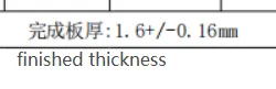
Figure 2: 1.6mm finished thickness
If ignored, this could have resulted in board warpage exceeding acceptable limits (per IPC-6012), leading to assembly issues, via cracking during reflow, or reduced reliability in field operation. The customer approved the adjusted stack, allowing us to proceed safely.
Non-Plated Hole with Hollow Solder Ring (NPTH Treatment)
The Gerber data showed a specific hole with a hollow solder ring opening. This configuration typically indicates a non-plated through hole (NPTH) requirement, but the exact treatment needed clarification. We asked whether the customer would accept standard no-copper hole processing.
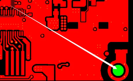
Figure 3: Hollow solder ring opening
Our CAM team identified this early because plating such holes unintentionally could cause shorting or assembly interference, while skipping plating without confirmation risks exposed copper edges after routing. If production continued without clarification, the risk included hole breakout during depanelization or poor mechanical strength at that location, potentially causing assembly failure when components are pressed in.
Silkscreen Legibility — Internal Text Too Small
We noticed several text elements inside the board outline were significantly undersized. After simulating the final white silkscreen on green solder mask, it became clear that these characters would be nearly unreadable post-fabrication.
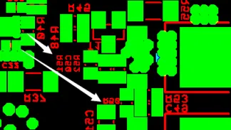
Figure 4: Undersized text elements
Our engineer raised this directly: "The board-internal font is too small and may not be clearly visible after production. We recommend confirming acceptance or increasing size where possible." Small silkscreen is a common DFM trigger — it not only affects traceability and assembly instructions but can also create cosmetic defects that fail IPC-A-600 Class 2 inspection. Ignoring this would likely result in customer rejection during incoming inspection or field service confusion.
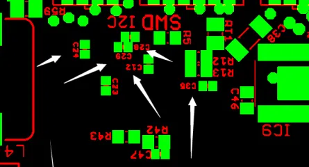
Figure 5: Small board-internal font
Process Edge Copper Addition for Current Balance
To improve etching uniformity and balance current distribution across the panel, our team proposed adding copper on the process edges. We asked for explicit confirmation before implementation.
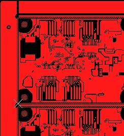
Figure 6: The panel and process edges
This is standard practice on panels with high copper density variation. Without it, we risked over-etching in low-density areas or under-etching elsewhere, leading to trace width reduction or shorts. The customer approved, preventing potential yield loss across the 8400-piece run.
Production Numbering and White Oil (Solder Mask) Handling
We also confirmed placement of added production serial numbers and clarified that no QR code was required in the white solder mask block, so standard block control would apply. These are lower-risk items but important for traceability.
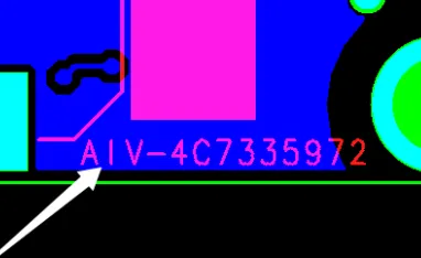
Figure 7: Added production serial numbers
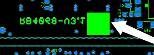
Figure 8: No QR code in the white solder mask block
Manufacturing Risks and DFM Insights
This case highlights several recurring DFM challenges in 4-layer designs. Stackup mismatches frequently cause warpage or delamination if resin flow and copper balance are not optimized. Small silkscreen features often fail readability requirements, while ambiguous hole treatments can lead to plating errors and mechanical weakness.
Process edge copper adjustments protect etching uniformity — critical for 6mil features. If these EQs had been ignored, consequences could include: board warpage leading to SMT placement failures, unreadable markings causing assembly errors, exposed copper near V-CUT lines resulting in edge shorting, or inconsistent hole plating causing open circuits or via cracking during thermal cycling.
Yield impact on a 700-set order would have been significant, with potential scrap rates climbing and delivery delays from rework cycles.
How the Engineering Team Resolved the Issues
Our engineering team worked quickly through the EQ list. We provided a revised lamination diagram, clear images of the proposed silkscreen simulation, and detailed drawings for the NPTH hole and process edge copper. After receiving customer approvals, we updated the CAM data, regenerated the production files, and confirmed all changes aligned with the original design intent.
"We adjusted the stackup to maintain electrical performance while ensuring mechanical stability," noted our CAM engineer. The panelization (including V-CUT and milling files) was also verified for clean depanelization without damaging critical features.
Final Manufacturing Outcome
All engineering questions were resolved with customer confirmation. The stackup was optimized, silkscreen adjustments noted where feasible, hole treatments standardized, and process enhancements applied. CAM review was completed and the order released for production within the agreed timeline. The job successfully moved forward without further delays.
Key Takeaways for PCB Designers
- Always provide clear, complete lamination stackup details including dielectric thicknesses and material references to avoid on-the-fly adjustments.
- Ensure silkscreen text height meets minimum 0.15–0.2mm for reliable readability on finished boards.
- Explicitly call out non-plated holes and special treatments in fabrication notes and Gerber files.
- Consider copper balance across the panel — factories may need to add process edge copper for etching stability.
- Separate V-CUT and milling files should be consistent with final panel dimensions and keep adequate clearance from active copper features.
- Review minimum feature sizes against the chosen manufacturer’s capabilities before tape-out.
- Respond promptly to EQs — early clarification prevents production halts and costly revisions.
FAQ
Q1: Why do factories adjust customer-provided stackups during CAM review?
A1: Customer stackups may not perfectly align with factory equipment and proven material flow characteristics. Adjustments ensure reliable lamination, controlled thickness, and reduced warpage risk while staying within the target finished board thickness.
Q2: What problems can arise from silkscreen text that is too small?
A2: Characters become illegible after processing, leading to assembly mistakes, traceability issues, or cosmetic rejection during quality inspection per IPC-A-600 standards.
Q3: Why ask for confirmation on non-plated hole (NPTH) treatment?
A3: Ambiguous hole treatment can result in unintended plating or incomplete copper removal, causing short circuits, mechanical weakness, or assembly interference.
Q4: What is the purpose of adding copper to process edges?
A4: It improves etching uniformity and current distribution across the panel, reducing the chance of over-etching fine traces or under-etching dense areas.
Q5: How critical is V-CUT clearance to exposed copper?
A5: Insufficient clearance risks exposed copper after scoring, which can cause edge shorting during handling or assembly. Factories often request confirmation or add protective measures.
Q6: Should designers always expect EQs on 4-layer boards?
A6: Not always, but detailed DFM review is standard. Even common builds can have subtle issues in stackup, panelization, or feature sizing that benefit from early engineering communication.