4-layer FR4 boards with customer-provided panelization frequently require intensive CAM review due to inconsistencies between supplied data and actual manufacturing requirements. This case reviews a real 4-layer order (105 × 209 mm, 1.6 mm thick, 1oz copper) where panel size mismatches, insufficient routing tabs, missing fiducials, and stackup documentation issues created multiple manufacturability risks. Our team raised targeted EQs to prevent panel breakage, registration problems during SMT, and production delays.
With 15+ years as a CAM engineer, I have handled countless similar cases where small panelization details lead to significant shop-floor problems. This article details the engineering questions we raised, the underlying manufacturing reasons, potential failure modes if ignored, and how clarification protected the build.
Order Overview
The project was a 4-layer FR4 PCB ( #FR4-20260325-108 ) using TG150 material and 1.6 mm finished thickness with 1oz copper throughout. Board size was 105 × 209 mm, panelized by the customer as 2×5. Surface finish was ENIG, with green solder mask and white legend. Minimum hole size was 0.3 mm, requiring 100% flying probe testing. Quantity was 100 pcs (10 sets). The design included routing separation and customer stackup documentation.
Customer self-panelization combined with tight tabs and missing process features made this order particularly sensitive to DFM validation before releasing to lamination and routing.
Main Engineering Questions Found During CAM Review
Panel Size Inconsistency Between Files and Attachments
We noticed conflicting panel dimensions: attachments showed 108 × 209 mm while actual Gerber data measured 105 × 209 mm. Our CAM team identified this early during file comparison. Accurate panel size is critical for correct routing programs and process edge definition.
Figure 1: conflicting panel dimensions
If ignored, mismatched dimensions could cause incorrect outline routing, misaligned tabs, or panels that do not fit production equipment. This often leads to scrap or rework. We asked the customer to confirm the correct size and updated files accordingly.
Insufficient Routing Tab Size (0.8 mm)
The original design specified only 0.8 mm wide tabs for panel connection. After reviewing the milling layer, our engineer determined this size was too narrow for stable production on a 4-layer 1.6 mm board. We recommended confirming or increasing tab width to prevent premature separation.
Figure 2: only 0.8 mm wide tabs for panel connection
If we had proceeded with 0.8 mm tabs, panels could break apart during routing, handling, or testing, causing board damage, misalignment, or complete loss of panels. We have seen narrow tabs result in high scrap rates and assembly line interruptions. The customer confirmed adjustments to ensure production stability.
Missing Locating Holes and Fiducials for SMT
The process edges lacked locating holes, and the board itself had no optical fiducials. Updated data showed optical points only on top and bottom but still no full set of locating features. Our production team flagged this because accurate panel registration is essential for SMT placement on multi-up panels.
Without proper fiducials and locating holes, SMT machines may experience placement errors, leading to component misalignment, solder defects, or rework. On a 2×5 panel, this risk multiplies across boards. We suggested adding standard locating holes and confirming fiducial placement.
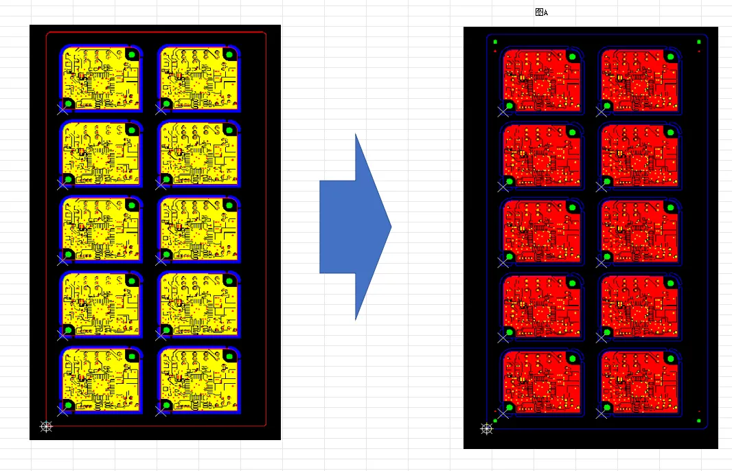
Figure 3: adding standard locating holes and confirming fiducial placement
Board Thickness and Stackup Confirmation
The updated customer data contained only a single stackup file with no additional attachments or detailed layer drawings. During our internal review, we identified this limitation and needed confirmation on the exact finished thickness tolerance. Our CAM engineer noted that we would proceed with manufacturing based on the provided stackup at 1.6 mm ±10% unless otherwise specified.
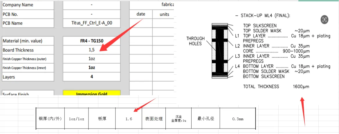
Figure 4: conflict regarding finished board thickness
We noticed the lack of comprehensive stackup details early in the file verification process. If left unconfirmed, proceeding with only a basic stackup file could lead to variations in dielectric thickness, resin flow issues during lamination, or final board thickness falling outside acceptable limits for the intended application. On a 1.6 mm 4-layer construction, such deviations might cause impedance inconsistencies, excessive bow and twist, or problems during downstream assembly and testing.
To reduce manufacturing risk, our engineering team requested explicit confirmation on the target finished thickness and any specific tolerances or layer arrangements. The customer’s clarification allowed us to lock in the parameters and proceed with confidence. This step is particularly important for multilayer boards where even small thickness variations can impact reliability under thermal stress or during press-fit connector assembly.
FAB Layer Copper Clearance and Markings
The customer requested UL marking and production cycle (week/year code) on the board, but no specific details were provided regarding exact content, font size, location, or layer placement. During CAM review of the legend and FAB layers, our team identified this gap as it directly affects traceability, regulatory compliance, and quality control. We needed the customer to confirm the precise UL logo/text format and the production week code format (typically YYWW) along with the preferred placement.
Our engineer recommended placing the UL mark and week code in a non-critical area of the top or bottom legend layer, ensuring sufficient clearance from components and copper features. After customer confirmation on content and position, we incorporated the markings into the production files. This clarification prevented potential compliance failures and ensured full traceability for the order. Such details, while seemingly minor, are critical for boards destined for industrial or certified applications.
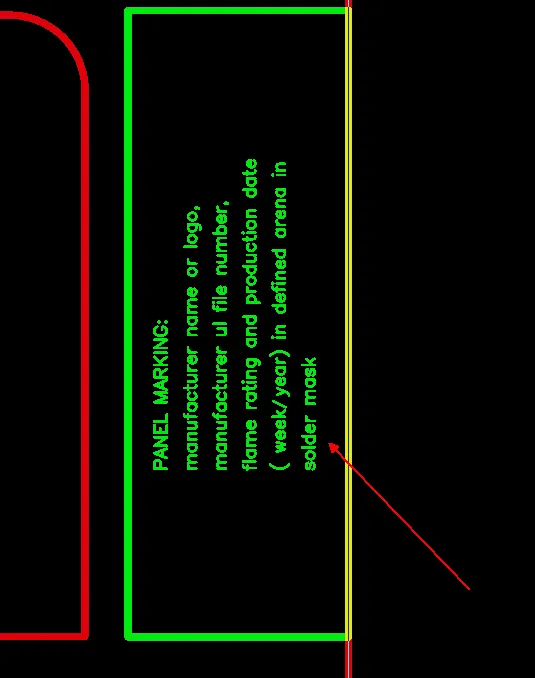
Figure 5: UL marking and production week code
Manufacturing Risks and DFM Insights
Customer self-panelization is a frequent source of EQs. Designers often underestimate the mechanical stresses during routing and handling, resulting in tabs that are too narrow. On 1.6 mm 4-layer boards, 0.8 mm tabs lack sufficient strength and can snap, scattering individual boards and damaging circuits.
Missing fiducials and locating holes directly impact downstream SMT yield. Inconsistent panel dimensions cause program errors in CNC routing. If these issues are ignored, consequences include panel breakage, registration failures, component placement defects, increased scrap, and missed delivery schedules. This case shows why clear communication on panelization details is essential before production.
How the Engineering Team Resolved the Issues
We sent a consolidated EQ list with marked-up images showing size differences, tab concerns, and missing features. After customer confirmation on the 105 × 209 mm panel size, increased tab dimensions, and addition of locating holes, our team updated the milling program and verified the stackup. FAB layer clearances were implemented, and standard markings were added.
These adjustments ensured panel stability and SMT compatibility while maintaining the original design intent.
Final Manufacturing Outcome
All engineering questions were resolved through customer confirmation. Production files were optimized, and the order was released for fabrication with updated panelization parameters.
Key Takeaways for PCB Designers
- Ensure all panelization files, attachments, and Gerbers share identical dimensions before submission.
- Design routing tabs with sufficient width (typically >1.5–2.0 mm depending on board thickness and layer count) to withstand production stresses.
- Include locating holes on process edges and optical fiducials on the board for reliable SMT processing on multi-up panels.
- Provide complete stackup documentation and confirm finished thickness expectations.
- Clearly define copper keep-out areas in the FAB layer and any required markings (UL, date code).
- Request DFM review when self-panelizing, especially for multilayer boards.
- Coordinate panel features with the fabricator early to avoid last-minute changes.
FAQ
Q1: Why are narrow routing tabs problematic in PCB panelization?
A1: Tabs under 1.0 mm often break during routing, depanelization, or handling, leading to loose boards, edge damage, and production scrap.
Q2: What is the risk of missing fiducials and locating holes?
A2: SMT machines rely on them for accurate alignment. Without them, component misplacement, solder defects, and rework become common, especially on multi-up panels.
Q3: Why do panel size mismatches trigger EQs?
A3: Conflicting dimensions between drawings and Gerbers lead to incorrect tooling programs, misrouted outlines, and panels that do not match production requirements.
Q4: How should designers prepare panelization data?
A4: Ensure consistency across all files, include adequate tabs, locating holes, and fiducials, and clearly communicate any special requirements in fabrication notes.
Q5: What is the recommended minimum tab size for 1.6 mm 4-layer panels?
A5: Generally 1.5–2.5 mm or wider depending on panel size and process. Manufacturers can advise based on specific equipment and material.