Introduction
This engineering case study examines a real 4-layer rigid-flex PCB order (#RFP-20251223-007) for a sensor application. Rigid-flex designs combine the mechanical flexibility of polyimide-based flex circuits with the stability of FR-4 rigid sections, making them ideal for compact, high-reliability electronics. However, they introduce significant manufacturing complexities due to differing material properties, transition zones, and process requirements.
During our standard CAM engineering review, multiple manufacturability issues surfaced that required clarification from the customer. These EQs (Engineering Questions) highlight common gaps between design intent and actual fabrication capabilities. In rigid-flex production, even small oversights in outline definition, via placement near flex areas, or stackup tolerances can lead to scrap, delamination, or assembly failures. Our goal with this case is to share practical insights that help designers avoid similar issues and reduce review cycles.
Order Overview
The project involved a 4-layer rigid-flex PCB with overall dimensions of approximately 133.69 mm × 160.84 mm, fabricated at 0.8 mm rigid board thickness. The order called for 20 pieces (10 sets) using ENIG surface finish, minimum hole size of 0.3 mm, and a 1x2 panelization arrangement. The design featured distinct rigid and flex regions, with PI stiffener reinforcement on the flex area for gold finger support. Testing was specified as full flying probe, with no blind/buried vias and standard IPC-II acceptance criteria. Delivery was requested within 7 days.
Key challenges included the hybrid construction: rigid sections used standard FR-4 processing while the flex portion required polyimide handling, selective coverlay, and precise control at the rigid-flex transition. The customer also specified single-piece shipping, dual-sided flex coverlay (yellow), matte black solder mask on rigid areas (top white silkscreen), and gold finger plating with specific Ni/Au thicknesses. These details demanded careful DFM validation before releasing to production.
Main Engineering Questions Found During CAM Review
Rigid-Flex Structure and Stackup Clarification
One of the first and most critical issues involved the stackup definition. The customer provided initial dimensions: rigid board thickness 0.8±0.08 mm, flex thickness 0.16±0.05 mm, with PI reinforcement bringing the flex area to 0.21 mm. After internal review, our engineer identified a mismatch with typical gold finger requirements. Single-row gold fingers generally target a total reinforced thickness around 0.3 mm for reliable connector mating and mechanical stability.
Figure 1: Rigid-flex board thickness with PI reinforcement
We noticed the PI stiffener specification of 0.2 mm conflicted with the desired total thickness. Our CAM team requested confirmation and later proposed an updated stackup achieving 0.3±0.05 mm in the reinforced flex region while maintaining 1 oz copper on inner and outer layers. If ignored, this could have resulted in gold fingers that were too thin, leading to poor contact reliability, bending fatigue, or connector insertion damage during assembly. According to common IPC-2221 guidelines for flex circuit construction, maintaining consistent thickness in reinforced areas is essential to prevent mechanical stress concentrations.
Figure 2: PI stiffener specification of 0.2 mm
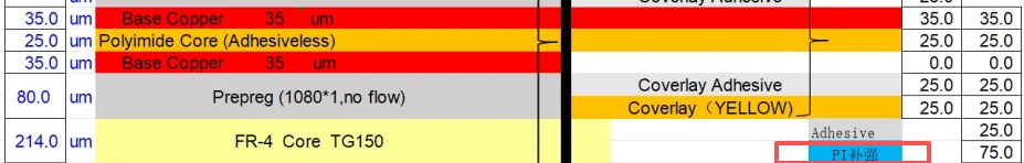
Figure 3: 0.3±0.05 mm in the reinforced flex region
Via Placement Near Flex Transition Zone
A significant DFM concern was the proximity of through-holes to the flex area. Multiple vias were positioned less than 0.6 mm from the rigid-flex boundary. In our experience, this is too close for reliable chemical processing. Our engineer suggested relocating these holes (original positions marked red, proposed blue) to ensure adequate clearance.

Figure 4: Proximity of through-holes to the flex area
If production had proceeded without adjustment, the vias could have allowed process chemicals to ingress into the flex polyimide layers during desmear, plating, or cleaning steps, causing contamination, delamination, or complete board scrap. We have seen cases where such proximity led to resin voids and open circuits after thermal stress. The adjustment was critical to protect yield in this hybrid construction.
Outline Modifications for Reliability
The rigid-flex transition outline presented another risk. Sharp internal corners in the flex-hard junction are prone to tearing during handling, routing, or assembly. Our team recommended changing these to a 0.5 mm radius (R angle), as shown in the production overlay. This is a standard practice in flex fabrication to distribute stress and prevent propagation of micro-tears into the copper layers.
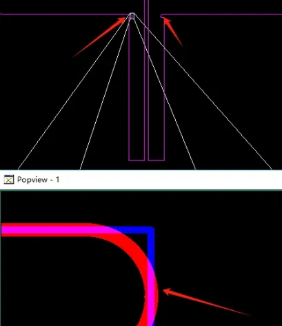
Figure 5: Recommended 0.5 mm radius (R angle)
Ignoring this would likely result in product tearing during depanelization or customer handling, leading to cosmetic defects and potential signal integrity issues if copper traces were affected. Our CAM engineer confirmed the modification after marking the proposed changes on the customer's data.
Gold Finger Clearance and Silkscreen Issues
To maintain adequate spacing between gold fingers and the board outline, we suggested trimming the fingers by 0.2 mm.

Figure 6: Suggested trimming the gold fingers by 0.2 mm
Additionally, the bottom-layer silkscreen data could not be properly processed. We asked the customer to confirm whether the bottom silkscreen should be omitted or to provide corrected files. We typically produce according to top-layer silkscreen unless otherwise specified.
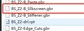
Figure 7: Unresolved bottom-layer silkscreen data
Unresolved silkscreen data could cause registration errors or incomplete legend application, while insufficient gold finger clearance risks edge plating exposure or shorting after contour routing.
Manufacturing Risks and DFM Insights
This case underscores several recurring DFM challenges in rigid-flex designs. Customers often underestimate the impact of transition zone geometry and via placement on process reliability. Without proper clearance, chemical ingress becomes a primary failure mode. Stackup mismatches frequently cause thickness-related assembly problems, especially with gold finger connectors. Sharp corners in flex outlines are a common source of mechanical failure.
If these EQs had been ignored, potential outcomes included: delamination at rigid-flex junctions, via cracking under thermal cycling, reduced yield from contamination, and field failures due to unreliable gold finger contacts. These issues typically trigger production delays, increased engineering communication, and higher scrap costs.
How the Engineering Team Resolved the Issues
Our engineering team provided marked-up production files highlighting all proposed changes. After receiving customer confirmations on the soft/hard area definitions, surface finish specs (ENIG with Au 2.0u″, Ni 120-200u″), single-piece shipping, and the updated stackup, we finalized the manufacturing data. The PI reinforcement was adjusted to achieve the target 0.3 mm thickness in the gold finger area. Outline modifications and via relocations were implemented in the CAM software. Bottom silkscreen was set to match top-layer intent pending final confirmation.
Throughout the process, we prioritized risk reduction while staying as close as possible to the original design intent. This collaborative approach ensured the files were fully manufacturable within our process capabilities.
Final Manufacturing Outcome
All engineering questions were resolved through customer confirmation. The stackup was optimized and approved, production files updated, and the order released for fabrication. The 4-layer rigid-flex boards proceeded with the adjusted parameters, maintaining the requested 7-day delivery timeline and IPC-II standards.
Key Takeaways for PCB Designers
- Always provide detailed rigid-flex stackup drawings with individual layer and reinforced zone thicknesses clearly specified.
- Maintain minimum clearances (typically ≥0.6 mm) between vias and flex transition zones to prevent chemical ingress.
- Incorporate fillet radii (minimum 0.5 mm) at internal corners of flex outlines to avoid tearing.
- Verify gold finger dimensions and stiffener thickness against connector requirements early in the design phase.
- Ensure consistent silkscreen data across layers and confirm any intentional omissions in fabrication notes.
- Use standard layer naming and include clear fabrication notes to reduce misinterpretation during CAM review.
- Consider panelization implications for rigid-flex boards, especially when requesting single-piece shipping.
FAQ
Q1: Why is via proximity to the rigid-flex transition zone a major concern?
A1: Vias placed too close (<0.6 mm) allow process chemicals to wick into the flex layers during plating and cleaning, risking contamination, delamination, and board scrap. Relocating vias provides necessary isolation.
Q2: What problems can sharp internal corners cause in flex circuits?
A2: Sharp corners concentrate mechanical stress, leading to tearing of the polyimide during routing, handling, or assembly. Adding a 0.5 mm radius distributes stress and significantly improves reliability.
Q3: Why adjust gold finger length and PI stiffener thickness?
A3: Proper dimensions ensure reliable connector mating and mechanical durability. A mismatch can cause insertion damage or poor electrical contact. We confirmed 0.3 mm total reinforced thickness as standard for single-row fingers.
Q4: What happens if stackup confirmation is skipped in rigid-flex production?
A4: Thickness variations can lead to assembly fit issues, impedance deviations, or mechanical weakness in the flex area, resulting in field failures or yield loss after thermal cycling.
Q5: Why do CAM engineers request clarification on silkscreen layers?
A5: Incomplete or conflicting silkscreen data can cause registration problems or unwanted legend printing. Confirming intent (e.g., top-only) prevents manufacturing errors and extra revision cycles.
Q6: How important is DFM review for rigid-flex PCBs?
A6: Extremely important. Hybrid constructions amplify risks from material differences. Early CAM review catches issues that could otherwise cause production delays, increased costs, or scrapped boards.